SBAS931B January 2019 – July 2022 ADS8353-Q1
PRODUCTION DATA
- 1Features
- 2Applications
- 3Description
- 4Revision History
- 5Pin Configuration and Functions
- 6Specifications
- 7Detailed Description
- 8Application and Implementation
- 9Device and Documentation Support
Package Options
Mechanical Data (Package|Pins)
- PW|16
Thermal pad, mechanical data (Package|Pins)
Orderable Information
8.1.1 Input Amplifier Selection
Selection criteria for the input amplifiers is highly dependent on the input signal type and the performance goals of the data acquisition system. Some key amplifier specifications to consider while selecting an appropriate amplifier to drive the inputs of the ADC are:
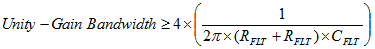
- Small-signal bandwidth. Select the small-signal bandwidth of the input amplifiers to be as high as possible after meeting the power budget of the system. Higher bandwidth reduces the closed-loop output impedance of the amplifier, thus allowing the amplifier to more easily drive the low cutoff frequency RC filter at the ADC inputs. Higher bandwidth also minimizes the harmonic distortion at higher input frequencies. Select the amplifier bandwidth as described in Equation 6 to maintain the overall stability of the input driver circuit:
Equation 6.
- Noise. Noise contribution of the front-end amplifiers must be as low as possible to prevent any degradation in SNR performance of the system. As a rule of thumb, to ensure that the noise performance of the data acquisition system is not limited by the front-end circuit, keep the total noise contribution from the front-end circuit below 20% of the input-referred noise of the ADC. Equation 7 calculates noise from the input driver circuit. This noise is band-limited by designing a low cutoff frequency RC filter:
Equation 7.
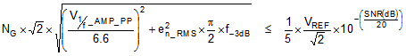
where:
- V1/f_AMP_PP = the peak-to-peak flicker noise in µV
- en_RMS = the amplifier broadband noise density in nV/√ Hz
- f–3dB = the 3-dB bandwidth of the RC filter
- NG = the noise gain of the front-end circuit, which is equal to 1 in a buffer configuration
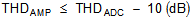
- Distortion. Both the ADC and the input driver introduce nonlinearity in a data acquisition block. As a rule of thumb, the distortion of the input driver must be at least 10 dB lower than the distortion of the ADC, as shown in Equation 8, to ensure that the distortion performance of the data acquisition system is not limited by the front-end circuit.
Equation 8.
- Settling Time. For dc signals with fast transients that are common in a multiplexed application, the input signal must settle to the desired accuracy at the inputs of the ADC during the acquisition time window. This condition is critical to maintain the overall linearity performance of the ADC. Typically, the amplifier data sheets specify the output settling performance only up to 0.1% to 0.001%, which may not be sufficient for the desired accuracy. Therefore, always verify the settling behavior of the input driver with TINA™-SPICE simulations before selecting the amplifier.