SLUS694G March 2006 – December 2014
PRODUCTION DATA.
- 1 Features
- 2 Applications
- 3 Description
- 4 Revision History
- 5 Device Comparison Table
- 6 Pin Configuration and Functions
- 7 Specifications
-
8 Detailed Description
- 8.1 Overview
- 8.2 Functional Block Diagram
- 8.3 Feature Description
- 8.4
Device Functional Modes
- 8.4.1 Sleep Mode - V(IN) < VI(BAT)
- 8.4.2 Standy Mode - V(IN) > VI(BAT)and CE (Chip Enable) Pin = Low
- 8.4.3
Battery Charge Mode - V(IN) > VI(BAT), Battery Present, CE pin = High and DPPM Pin Not Floating
- 8.4.3.1 Automous Power Selection and Boot-Up Sequence
- 8.4.3.2 Charge Control
- 8.4.3.3 Battery Preconditioning
- 8.4.3.4 Battery Charge Current
- 8.4.3.5 Battery Voltage Regulation
- 8.4.3.6 Temperature Regulation and Thermal Protection
- 8.4.3.7 Charge Timer Operation
- 8.4.3.8 Timer Fault Recovery
- 8.4.3.9 Charge Termination and Recharge
- 9 Application and Implementation
- 10Power Supply Recommendations
- 11Layout
- 12Device and Documentation Support
- 13Mechanical, Packaging, and Orderable Information
Package Options
Refer to the PDF data sheet for device specific package drawings
Mechanical Data (Package|Pins)
- RHL|20
Thermal pad, mechanical data (Package|Pins)
- RHL|20
Orderable Information
9 Application and Implementation
NOTE
Information in the following applications sections is not part of the TI component specification, and TI does not warrant its accuracy or completeness. TI’s customers are responsible for determining suitability of components for their purposes. Customers should validate and test their design implementation to confirm system functionality.
9.1 Application Information
Compared to chargers without dynamic power path management (DPPM), this single-cell LiIon battery charger provides instant system power even with a deeply discharged battery. The maximum charge current is set by ISET2 but the input current limit circuitry, controlled by ISET1 and MODE pins or the DPPM circuitry can reduce the charge current from the maximum desired value.
9.2 Typical Application
 Figure 7. Typical Application Circuit
9.2.1 Design Requirements
A bq24070 (VOUT = 4.4 Vreg) is powered through an AC adaptor with IN input is set for approximately 5.1 V (1.5 A current limit), I(CHG) = 1 A, V(DPPM-SET) = 3.7 V, V(DPPM-REG) = 1.15 × V(DPPM-SET) = 4.26 V, Mode = H, and USB input is not connected. A 103AT thermistor is inside the battery pack. A 6-hour saftey time-out is desired.
9.2.2 Detailed Design Procedure
The minimum required 0.1 μF capacitors are placed on IN and OUT. Additional 10-μF capacitors are included on IN and OUT to improve load transient response. The recommended (but not required) 33-μF capacitor on BAT is added to allow for operation when no battery is attached. A 0.22-μF capacitor is connected between BAT and ISET1 to improve operation at low charge currents.
Rearranging Equation 4 gives RSET = V(SET) x K(SET) / IO(BAT) = 2.5 V x 425 / 1 A = 1062.5 Ω → 1070 Ω. Per Equation 3, the precharge current is 100 mA and per Equation 8, the termination current is 100 mA. Since MODE is high, in order to prevent the charge current from being reduced by 1/2, ISET2 is tied high.
Rearranging Equation 5 gives RTMR = t(CHG) / K(TMR) gives 6 hrs x 60 min/hr x 60 s/min / 0.360 s/Ω = 60 kΩ → 60.4 kΩ
Rearranging Equation 1 gives RDPPM = V(DPPM-REG) / (I(DPPM) x SF) = 4.26 V / ( 100 μA x 1.15) = 37.044 kΩ →37.4 kΩ. CDPPM of 10 nF was added to prevent the IC from falsely entering short circuit protection at start-up.
Not shown are 1.5-kΩ resistors and LEDs pulled up to V(IN) from STAT1, STAT2, and PG.
9.2.2.1 Selecting the Input and Output Capacitors
In most applications, all that is needed is a high-frequency decoupling capacitor on the input. A 0.1-μF ceramic capacitor placed in close proximity to the IN to VSS pins works well. In some applications, depending on the power-supply characteristics and cable length, adding an additional 4.7-μF to 10-μF ceramic capacitor to the input might be required.
The bq2407x requires only a small output capacitor for loop stability. A 0.1-μF ceramic capacitor placed between the OUT and VSS pin is typically sufficient. TI recommends installing at least an additional 10-uF ceramic capacitor between OUT and VSS in order to improve load transient response.
TI recommends installing a minimum 33-μF capacitor between the BAT pin and VSS (in parallel with the battery). This configuration ensures proper hot-plug power up with a no-load condition (no system load or battery attached).
VREF output capacitor with a value of 0.1 μF is required. A 0.22-μF capacitor connected between BAT and ISET1 is recommended to improve operation at low charge currents.
This short-circuit disable feature was implemented mainly for power up when inserting a battery. Because the BAT input voltage rises much faster than the OUT voltage (Vout<Vbat-200 mV), with most any capacitive load on the output, the part can get stuck in short-circuit mode. Placing a 1-nF to 100-nF capacitor between the DPPM pin and ground slows the VDPPM rise time, during power up, and delays the short-circuit protection.
9.2.3 Application Curves
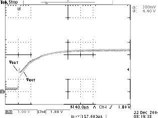 Figure 8. Insert Battery – Power-Up Output through BAT
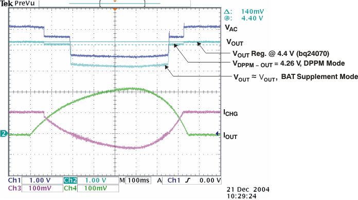 Figure 10. DPPM and Battery Supplement Modes
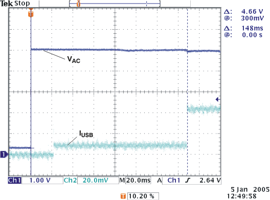 Figure 9. USB Boot-Up Power-Up