SLUS694G March   2006  – December 2014

PRODUCTION DATA.  

  1. Features
  2. Applications
  3. Description
  4. Revision History
  5. Device Comparison Table
  6. Pin Configuration and Functions
  7. Specifications
    1. 7.1 Absolute Maximum Ratings
    2. 7.2 ESD Ratings
    3. 7.3 Recommended Operating Conditions
    4. 7.4 Thermal Information
    5. 7.5 Electrical Characteristics
    6. 7.6 Typical Characteristics
  8. Detailed Description
    1. 8.1 Overview
    2. 8.2 Functional Block Diagram
    3. 8.3 Feature Description
      1. 8.3.1 Power-Path Management
        1. 8.3.1.1 Case 1: IN Mode (Mode = High)
          1. 8.3.1.1.1 System Power
          2. 8.3.1.1.2 Charge Control
          3. 8.3.1.1.3 Dynamic Power-Path Management (DPPM)
        2. 8.3.1.2 Case 2: USB Mode (Mode = L)
          1. 8.3.1.2.1 System Power
          2. 8.3.1.2.2 Charge Control
          3. 8.3.1.2.3 Dynamic Power-Path Management (DPPM)
          4. 8.3.1.2.4 Application Curve Descriptions
      2. 8.3.2 Battery Temperature Monitoring
      3. 8.3.3 Charge Status Outputs
      4. 8.3.4 PG, Outputs (Power Good)
      5. 8.3.5 Short-Circuit Recovery
      6. 8.3.6 VREF
    4. 8.4 Device Functional Modes
      1. 8.4.1 Sleep Mode - V(IN) < VI(BAT)
      2. 8.4.2 Standy Mode - V(IN) > VI(BAT)and CE (Chip Enable) Pin = Low
      3. 8.4.3 Battery Charge Mode - V(IN) > VI(BAT), Battery Present, CE pin = High and DPPM Pin Not Floating
        1. 8.4.3.1 Automous Power Selection and Boot-Up Sequence
        2. 8.4.3.2 Charge Control
        3. 8.4.3.3 Battery Preconditioning
        4. 8.4.3.4 Battery Charge Current
        5. 8.4.3.5 Battery Voltage Regulation
        6. 8.4.3.6 Temperature Regulation and Thermal Protection
        7. 8.4.3.7 Charge Timer Operation
        8. 8.4.3.8 Timer Fault Recovery
        9. 8.4.3.9 Charge Termination and Recharge
  9. Application and Implementation
    1. 9.1 Application Information
    2. 9.2 Typical Application
      1. 9.2.1 Design Requirements
      2. 9.2.2 Detailed Design Procedure
        1. 9.2.2.1 Selecting the Input and Output Capacitors
      3. 9.2.3 Application Curves
  10. 10Power Supply Recommendations
  11. 11Layout
    1. 11.1 Layout Guidelines
    2. 11.2 Layout Example
    3. 11.3 Thermal Considerations
  12. 12Device and Documentation Support
    1. 12.1 Documentation Support
      1. 12.1.1 Related Documentation
    2. 12.2 Related Links
    3. 12.3 Trademarks
    4. 12.4 Electrostatic Discharge Caution
    5. 12.5 Glossary
  13. 13Mechanical, Packaging, and Orderable Information

Package Options

Refer to the PDF data sheet for device specific package drawings

Mechanical Data (Package|Pins)
  • RHL|20
Thermal pad, mechanical data (Package|Pins)
Orderable Information

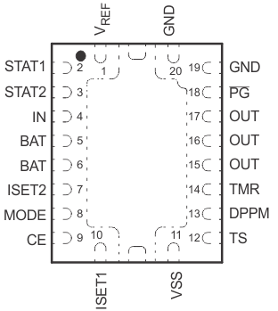
6 Pin Configuration and Functions

RHL Package
20 Pins
Top View
po_lus694.gif

Pin Functions

PIN I/O DESCRIPTION
NAME NO.
BAT 5, 6 I/O Battery input and output.
CE 9 I Chip enable input (active high)
DPPM 13 I Dynamic power-path management set point (account for scale factor)
GND 19, 20 I Ground input
IN 4 I Charge input voltage
ISET1 10 I/O Charge current set point and precharge and termination set point
ISET2 7 I Charge current set point for USB port. (High = 500 mA, Low = 100 mA) See half-charge current mode using ISET2.
MODE 8 I Power source selection input (Low for USB mode current limit)
OUT 15, 16, 17 O Output terminal to the system
PG 18 O Power-good status output (open-drain)
STAT1 2 O Charge status output 1 (open-drain)
STAT2 3 O Charge status output 2 (open-drain)
TMR 14 I/O Timer program input programmed by resistor. Disable fast-charge safety timer and termination by tying TMR to VREF.
TS 12 I/O Temperature sense input
VREF 1 O Internal reference signal
VSS 11 Ground input (the thermal pad on the underside of the package) There is an internal electrical connection between the exposed thermal pad and VSS pin of the device. The exposed thermal pad must be connected to the same potential as the VSS pin on the printed-circuit board. Do not use the thermal pad as the primary ground input for the device. VSS pin must be connected to ground at all times.