SLUSBY5G June 2014 – December 2015
UNLESS OTHERWISE NOTED, this document contains PRODUCTION DATA.
- 1 Features
- 2 Applications
- 3 Description
- 4 Revision History
- 5 Pin Configuration and Functions
- 6 Specifications
-
7 Detailed Description
- 7.1 Overview
- 7.2 Functional Block Diagram
- 7.3 Feature Description
- 7.4
Device Functional Modes
- 7.4.1 High Impedance Mode
- 7.4.2 Battery Only Connected
- 7.4.3 Input Connected
- 7.4.4 Battery Charging Process
- 7.4.5 Charge Time Optimizer
- 7.4.6 Battery Detection
- 7.4.7 Battery Overvoltage Protection (BOVP)
- 7.4.8 Dynamic Power Path Management
- 7.4.9 Battery Discharge FET (BGATE)
- 7.4.10 IUSB1, IUSB2, and IUSB3 Input
- 7.4.11 Safety Timer in Charge Mode
- 7.4.12 LDO Output (DRV)
- 7.4.13 External NTC Monitoring (TS)
- 7.4.14 Thermal Regulation and Protection
- 7.4.15 Status Outputs (CHG, PG)
- 7.4.16 Boost Mode Operation
- 8 Applications and Implementation
- 9 Power Supply Recommendations
- 10Layout
- 11Device and Documentation Support
- 12Mechanical, Packaging, and Orderable Information
Package Options
Mechanical Data (Package|Pins)
- RGE|24
Thermal pad, mechanical data (Package|Pins)
Orderable Information
10 Layout
10.1 Layout Guidelines
The following provides some guidelines:
- Place 1µF input capacitor as close to PMID pin and PGND pin as possible to make high frequency current loop area as small as possible.
- Connect the GND of the PMID and IN caps as close as possible.
- Place 4.7µF input capacitor as close to IN pin and PGND pin as possible to make high frequency current loop area as small as possible.
- The local bypass capacitor from SYS to GND should be connected between the SYS pin and PGND of the IC. The intent is to minimize the current path loop area from the SW pin through the LC filter and back to the PGND pin.
- Place all decoupling capacitors close to their respective IC pin and as close as to PGND as possible. Do not place components such that routing interrupts power stage currents. All small control signals should be routed away from the high current paths.
- The PCB should have a ground plane (return) connected directly to the return of all components through vias. Two vias per capacitor for power-stage capacitors and one via per capacitor for small-signal components. It is also recommended to put vias inside the PGND pads for the IC, if possible. A star ground design approach is typically used to keep circuit block currents isolated (high-power/low-power small-signal) which reduces noise-coupling and ground-bounce issues. A single ground plane for this design gives good results.
- The high-current charge paths into IN, BAT, SYS and from the SW pins must be sized appropriately for the maximum charge current in order to avoid voltage drops in these traces. The PGND pins should be connected to the ground plane to return current through the internal low-side FET.
- For high-current applications, the balls for the power paths should be connected to as much copper in the board as possible. This allows better thermal performance as the board pulls heat away from the IC.
10.2 Layout Example
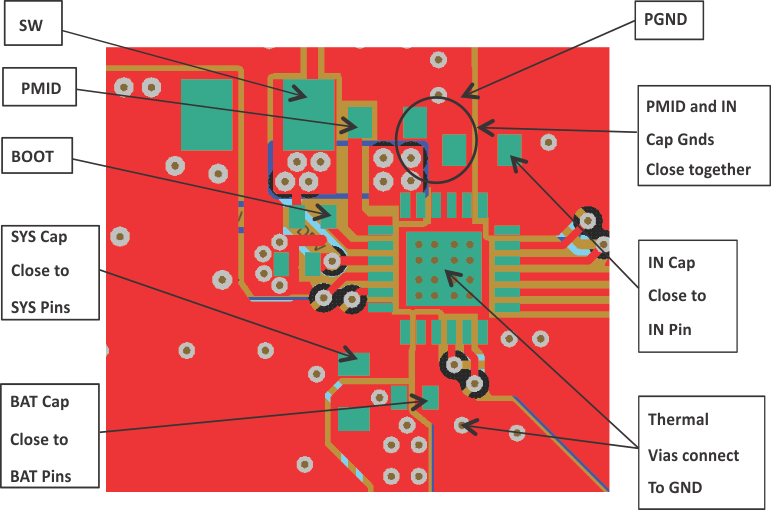
It is important to pay special attention to the PCB layout. Figure 30 provides a sample layout for the high current paths of the bq24266RGE.
 Figure 30. Recommended bq24266 PCB Layout for QFN Package
spacer