SLUSBY5G June   2014  – December 2015

UNLESS OTHERWISE NOTED, this document contains PRODUCTION DATA.  

  1. Features
  2. Applications
  3. Description
  4. Revision History
  5. Pin Configuration and Functions
  6. Specifications
    1. 6.1 Absolute Maximum Ratings
    2. 6.2 ESD Ratings
    3. 6.3 Recommended Operating Conditions
    4. 6.4 Thermal Information
    5. 6.5 Electrical Characteristics
    6. 6.6 Switching Characteristics
    7. 6.7 Typical Characteristics
  7. Detailed Description
    1. 7.1 Overview
    2. 7.2 Functional Block Diagram
    3. 7.3 Feature Description
    4. 7.4 Device Functional Modes
      1. 7.4.1  High Impedance Mode
      2. 7.4.2  Battery Only Connected
      3. 7.4.3  Input Connected
        1. 7.4.3.1 Input Voltage Protection in Charge Mode
          1. 7.4.3.1.1 Sleep Mode
          2. 7.4.3.1.2 Input Voltage Based Dynamic Power Management (VIN-DPM)
          3. 7.4.3.1.3 Input Overvoltage Protection
        2. 7.4.3.2 Charge Profile
      4. 7.4.4  Battery Charging Process
      5. 7.4.5  Charge Time Optimizer
      6. 7.4.6  Battery Detection
      7. 7.4.7  Battery Overvoltage Protection (BOVP)
      8. 7.4.8  Dynamic Power Path Management
      9. 7.4.9  Battery Discharge FET (BGATE)
      10. 7.4.10 IUSB1, IUSB2, and IUSB3 Input
      11. 7.4.11 Safety Timer in Charge Mode
      12. 7.4.12 LDO Output (DRV)
      13. 7.4.13 External NTC Monitoring (TS)
      14. 7.4.14 Thermal Regulation and Protection
      15. 7.4.15 Status Outputs (CHG, PG)
      16. 7.4.16 Boost Mode Operation
        1. 7.4.16.1 PWM Controller in Boost Mode
        2. 7.4.16.2 Burst Mode during Light Load
        3. 7.4.16.3 CHG and PG During Boost Mode
        4. 7.4.16.4 Protection in Boost Mode
          1. 7.4.16.4.1 Output Over-Voltage Protection
          2. 7.4.16.4.2 Output Over-Current Protection
          3. 7.4.16.4.3 Battery Voltage Protection
  8. Applications and Implementation
    1. 8.1 Application Information
    2. 8.2 Typical Applications
      1. 8.2.1 Typical Application, External Discharge FET
        1. 8.2.1.1 Design Requirements
        2. 8.2.1.2 Detailed Design Procedure
          1. 8.2.1.2.1 Output Inductor and Capacitor Selection Guidelines
      2. 8.2.2 Application Curves
  9. Power Supply Recommendations
    1. 9.1 Requirements for SYS Output
    2. 9.2 Requirements for Charging
  10. 10Layout
    1. 10.1 Layout Guidelines
    2. 10.2 Layout Example
  11. 11Device and Documentation Support
    1. 11.1 Documentation Support
      1. 11.1.1 Related Documentation
    2. 11.2 Related Links
    3. 11.3 Community Resources
    4. 11.4 Trademarks
    5. 11.5 Electrostatic Discharge Caution
    6. 11.6 Glossary
  12. 12Mechanical, Packaging, and Orderable Information

Package Options

Mechanical Data (Package|Pins)
Thermal pad, mechanical data (Package|Pins)
Orderable Information

6 Specifications

6.1 Absolute Maximum Ratings(1)

over operating free-air temperature range (unless otherwise noted)
VALUE UNIT
MIN MAX
Pin Voltage (with respect to PGND) IN –1.3 30 V
BOOT, PMID –0.3 30
SW –0.7 20
BAT –0.3 5
DRV, BGATE, CE, ISET, IUSB1, IUSB2, IUSB3, PG, CHG, SYS, TS –0.3 5.5
AGND -0.3 0.3
BOOT to SW –0.3 5 V
Output Current (Continuous) SW 4.5 A
SYS, BAT (charging/ discharging) 3.5
Input Current (Continuous) 2.75 A
Output Sink Current CHG, PG 10 mA
Operating free-air temperature –40 85 °C
Junction temperature, TJ –40 125
Storage temperature, Tstg 300 °C
(1) Stresses beyond those listed under absolute maximum ratings may cause permanent damage to the device. These are stress ratings only, and functional operation of the device at these or any other conditions beyond those indicated under recommended operating conditions is not implied. Exposure to absolute-maximum-rated conditions for extended periods may affect device reliability. All voltage values are with respect to the network ground pin unless otherwise noted.

6.2 ESD Ratings

VALUE UNIT
V(ESD) Electrostatic discharge Human body model (HBM), per ANSI/ESDA/JEDEC JS-001, all pins(1) ±2000 V
Charged device model (CDM), per JEDEC specification JESD22-C101, all pins(2) ±500 V
(1) JEDEC document JEP155 states that 500-V HBM allows safe manufacturing with a standard ESD control process.
(2) JEDEC document JEP157 states that 250-V CDM allows safe manufacturing with a standard ESD control process.

6.3 Recommended Operating Conditions

over operating free-air temperature range (unless otherwise noted)
MIN NOM MAX UNIT
VIN IN voltage range 4.2 13.5(1) V
IN operating voltage range 4.2 14
IIN Input current, IN input 2.5 A
ISW Output Current from SW, DC 3 A
IBAT, ISYS Charging 3 A
Discharging, using internal battery FET 3
TJ Operating junction temperature range 0 125 °C
(1) The inherent switching noise voltage spikes should not exceed the absolute maximum rating on either the BOOT or SW pins. A tight layout minimizes switching noise.

6.4 Thermal Information

THERMAL METRIC(1) bq24266 UNIT
RGE
(24 PINS)
RθJA Junction-to-ambient thermal resistance 32.6 °C/W
RθJC(top) Junction-to-case (top) thermal resistance 30.5 °C/W
RθJB Junction-to-board thermal resistance 3.3 °C/W
ψJT Junction-to-top characterization parameter 0.4 °C/W
ψJB Junction-to-board characterization parameter 9.3 °C/W
RJC(bot) Junction-to-case (bottom) thermal resistance 2.6 °C/W
(1) For more information about traditional and new thermal metrics, see the IC Package Thermal Metrics application report, SPRA953.

6.5 Electrical Characteristics

Circuit of , VUVLO < VIN < VOVP AND VIN > VBAT+ VSLP, TJ = –40°C to 125°C and TJ = 25°C for typical values (unless otherwise noted)
PARAMETER TEST CONDITIONS MIN TYP MAX UNIT
INPUT CURRENTS
IIN Supply current for control VUVLO < VIN < VOVP and VIN>VBAT+VSLP
PWM switching
15 mA
VUVLO < VIN < VOVP and VIN>VBAT+VSLP
PWM NOT switching
6.65
0°C< TJ < 85°C, VIN = 5V, High-Z Mode 250 μA
IBAT_HIZ Battery discharge current in High Impedance mode, (BAT, SW, SYS) 0°C< TJ < 85°C, VBAT = 4.2 V, VIN = 5V,
SCL, SDA = 0V or 1.8V, High-Z Mode
15 μA
0°C< TJ < 85°C, VBAT = 4.2 V, VIN = 0V,
SCL, SDA = 0V or 1.8V
80
POWER-PATH MANAGEMENT
VSYSREG(LO) System Regulation Voltage VBAT < VMINSYS, battery attached VMINSYS
+ 80mV
VMINSYS
+ 100mV
VMINSYS
+ 120mV
V
VSYSREG(HI) System Regulation Voltage Battery FET turned off, no charging,
VBAT > 3.5V
VBATREG
+2.2%
VBATREG
+2.5%
VBATREG
+2.77%
V
VMINSYS Minimum System Voltage Regulation Threshold VBAT + VDO(SYS_BAT) < 3.5V 3.44 3.5 3.55 V
tDGL(MINSYS_CMP) Deglitch time, VMINSYS comparator rising 8 ms
VBSUP1 Enter supplement mode threshold VBAT > VBUVLO VBAT – 20mV V
VBSUP2 Exit supplement mode threshold VBAT > VBUVLO VBAT – 5mV V
ILIM(DISCH) Current Limit, Discharge or Supplement Mode VLIM(BGATE) = VBAT – VSYS 4 6 A
tDGL(SC1) Deglitch Time, OUT Short Circuit during Discharge or Supplement Mode Measured from IBAT = 7A to FET off 250 μs
tREC(SC1) Recovery time, OUT Short Circuit during Discharge or Supplement Mode 2 s
Battery Range for BGATE Operation 2.5 4.5 V
BATTERY CHARGER
RON(BAT-SYS) Internal battery charger MOSFET on-resistance Measured from BAT to SYS,
VBAT = 4.2V, High-Z mode
32 47
VBATREG Charge Voltage TJ = 25°C 4.18 4.2 4.22 V
Charge Voltage TJ = 0°C to 85°C 4.17 4.2 4.23 V
Charge Voltage TJ = 0°C to 85°C, TS WARM 4.03 4.06 4.09 V
Voltage Regulation Accuracy TJ = 0°C to 125°C -1.0% 1.0%
ICHARGE Fast Charge Current Range VBATSHRT ≤ VBAT < VBAT(REG) 500 3000 mA
Fast Charge Current Accuracy 500 mA ≤ ICHARGE ≤ 1A –10% 10%
ICHARGE > 1000 mA –5% 5%
KISET Programmable Fast Charge Current Factor CE1=X, CE2=0, ICHARGE > 1000 mA 1140 1200 1260
CE1=X, CE2=0, 500 mA ≤ ICHARGE ≤ 1A 1080 1200 1320
TS COOL, ICHARGE > 1000 mA 570 600 630
TS COOL, 500 mA ≤ ICHARGE ≤ 1A 540 600 660
VBATSHRT Battery short circuit threshold 2.9 3 3.1 V
VBATSHRT_HYS Hysteresis for VBATSHRT Battery voltage falling 100 mV
Deglitch time for battery short to fastcharge transition VBAT rising or falling 1 ms
IBATSHRT Battery short circuit charge current VBAT < VBATSHRT 33.5 .50 66.5 mA
ITERM Termination charge current 50mA ≤ ITERM ≤ 300 mA 10 % of ICHARGE
Termination charge current accuracy ITERM ≤ 50 mA –30% 30%
50 mA < ITERM < 200 mA –15% 15%
ITERM ≥ 200 mA –15% 10%
tDGL(TERM) Deglitch time for charge termination Both rising and falling, 2-mV over-drive,
tRISE, tFALL=100ns
32 ms
VRCH Recharge threshold voltage Below VBATREG 100 120 150 mV
tDGL(RCH) Deglitch time VBAT falling below VRCH, tFALL=100ns 32 ms
VDET(SRC1) Battery detection voltage threshold
(TE = 1)
During current source (Turn IBATSHRT off) VRCH V
VDET(SRC2) During current source (Turn IBATSHRT on) VRCH
– 200mV
V
VDET(SNK) During current sink VBATSHRT V
IDETECT Battery detection current before charge done (sink current) Termination enabled (TE = 1) 7 mA
tDETECT(SRC) Battery detection time (sourcing current) Termination enabled (TE = 1) 2 s
tDETECT(SNK) Battery detection time (sinking current) Termination enabled (TE = 1) 250 ms
INPUT CURRENT LIMITING
IINLIM Input current limiting threshold USB charge mode, VIN = 5V, Current pulled from SW IINLIM=USB100 90 95 100 mA
IINLIM=USB500 450 475 500
IINLIM=USB150 125 140 150
IINLIM=USB900 800 850 900
IINLIM=1.5A 1425 1500 1575
IINLIM=2.5A 2225 2500 2825
VIN_DPM Input based DPM threshold range Charge mode, programmable via VDPM 4.2 11.6 V
VVDPM Feedback threshold 1.15 1.2 1.25 V
VDRV BIAS REGULATOR
VDRV Internal bias regulator voltage VIN>5V 4.3 4.8 5.3 V
IDRV DRV Output Current 0 10 mA
VDO_DRV DRV Dropout Voltage
(VIN – VDRV)
IIN = 1A, VIN = 4.2V, IDRV = 10mA 450 mV
STATUS OUTPUT (PG, CHG)
VOL Low-level output saturation voltage IO = 10 mA, sink current 0.4 V
IIH High-level leakage current V PG = V CHG = 5V 1 µA
INPUT PINS (CE1, CE2, IUSB1, IUSB2, IUSB3)
VIL Input low threshold 0.4 V
VIH Input high threshold 1.4 V
RPULLDOWN 100
PROTECTION
VUVLO IC active threshold voltage VIN rising 3.2 3.3 3.4 V
VUVLO_HYS IC active hysteresis VIN falling from above VUVLO 300 mV
VBATUVLO Battery Undervoltage Lockout threshold VBAT falling, VIN>VUVLO 2.4 2.6 V
VSLP Sleep-mode entry threshold, VIN-VBAT 2.0 V < VBAT < VBATREG, VIN falling 0 40 120 mV
tDGL(BAT) Deglitch time, BAT above VBATUVLO before SYS starts to rise 1.2 ms
VSLP_HYS Sleep-mode exit hysteresis VIN rising above VSLP 40 100 190 mV
tDGL(VSLP) Deglitch time for supply rising above VSLP+VSLP_HYS Rising voltage, 2-mV over drive, tRISE=100ns 30 ms
VOVP Input supply OVP threshold voltage IN rising, 100mV hysteresis 13.6 14 14.4 V
tDGL(BUCK_OVP) Deglitch time, VIN OVP in Buck Mode IN falling below VOVP 30 ms
VBOVP Battery OVP threshold voltage VBAT threshold over VOREG to turn off charger during charge 1.03 ×
VBATREG
1.05 ×
VBATREG
1.07 ×
VBATREG
V
VBOVP_HYS VBOVP hysteresis Lower limit for VBAT falling from above VBOVP 1 % of VBATREG
tDGL(BOVP) BOVP Deglitch Battery entering/exiting BOVP 8 ms
ICbCLIMIT Cycle-by-cycle current limit VSYS shorted 4.1 4.5 4.9 A
TSHTDWN Thermal trip 150 °C
Thermal hysteresis 10 °C
TREG Thermal regulation threshold Input current begins to cut off 125 °C
Safety Timer Time 29160 32400 35640 s
PWM
RDSON_Q1 Internal top MOSFET on-resistance Measured from IN to SW 80 135
RDSON_Q2 Internal bottom N-channel MOSFET on-resistance Measured from SW to PGND 80 135
fOSC Oscillator frequency 1.35 1.5 1.65 MHz
DMAX Maximum duty cycle 95%
DMIN Minimum duty cycle 0%
BATTERY-PACK NTC MONITOR
VHOT High temperature threshold VTS falling, 2% VDRV Hysteresis 27.3 30 32.6 %VDRV
VWARM Warm temperature threshold VTS falling, 2% VDRV Hysteresis 36.0 38.3 41.2 %VDRV
VCOOL Cool temperature threshold VTS rising, 2% VDRV Hysteresis 54.7 56.4 58.1 %VDRV
VCOLD Low temperature threshold VTS rising, 2% VDRV Hysteresis 58.2 60 61.8 %VDRV
TSOFF TS Disable threshold VTS rising, 4% VDRV Hysteresis 80 85 %VDRV
tDGL(TS) Deglitch time on TS change Applies to VHOT, VWARM, VCOOL and VCOLD 50 ms
OTG BOOST SUPPLY
IQBAT_ BOOST Quiescent current during boost mode (BAT pin) 3.3V<VBAT<4.5V, no switching 100 µA
Battery voltage range for specified boost operation VBAT falling 3.3 4.5 V
VIN_BOOST Boost output voltage (to pin VBUS) 3.3V<VBAT<4.5V over line and load 4.95 5.05 5.2 V
IBO Maximum output current for boost 3.3V<VBAT<4.5V BOOST_ILIM = 1 1000 mA
BOOST_ILIM = 0 500
IBLIMIT Cycle by cycle current limit for boost (measured at low-side FET) 3.3V<VBAT<4.5V BOOST_ILIM = 1 4 A
BOOST_ILIM = 0 2
VBOOSTOVP Over voltage protection threshold for boost (IN pin) Signals fault and exits boost mode 5.8 6 6.2 V
tDGL(BOOST_OVP) Deglitch Time, VIN OVP in Boost Mode 170 µs
VBURST(ENT) Upper VIN voltage threshold to enter burst mode (stop switching) 5.1 5.2 5.3 V
VBURST(EXIT) Lower VBUS voltage threshold to exit burst mode (start switching) 4.9 5 5.1 V

6.6 Switching Characteristics

over operating free-air temperature range (unless otherwise noted)
PARAMETER TEST CONDITIONS MIN TYP MAX UNIT
fOSC Oscillator frequency 1.35 1.5 1.65 Mhz
DMAX Maximum duty cycle 95%
DMIN Minimum duty cycle 0%

6.7 Typical Characteristics

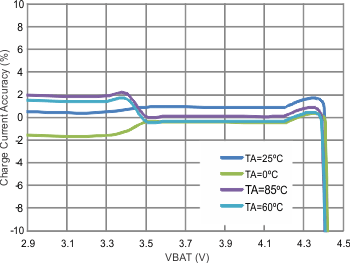
bq24266 charge_curr_v_VBAT_SLUSBA2.gif Figure 1. Charge Current vs Battery Voltage
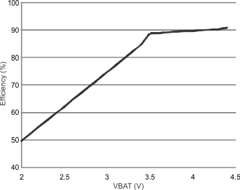
bq24266 efficiency_v_VBAT_SLUSBA2.gif Figure 3. Efficiency vs Battery Voltage
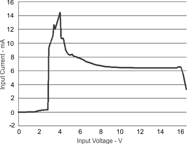
bq24266 viniq_nobat_nosys_SLUSBK7.gif Figure 5. Input IQ - No Battery, No System
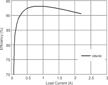
bq24266 vsys_eff_load_curr_SLUSBY5.gif Figure 2. Efficiency vs Output Current
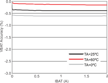
bq24266 vbat_accur42v_ibat_slusbk7.gif Figure 4. VBAT Accuracy vs IBAT – 4.2 VBAT
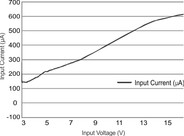
bq24266 viniq_hiz_nobat_nosys_SLUSBK7.gif Figure 6. Input IQ with Hi-Z Enabled