SLUSBD1B MARCH 2013 – September 2016
PRODUCTION DATA.
- 1 Features
- 2 Applications
- 3 Description
- 4 Pin Configuration and Function
- 5 Specifications
-
6 Detailed Description
- 6.1 Overview
- 6.2 Functional Block Diagram
- 6.3
Feature Description
- 6.3.1 Switching Frequency Adjust
- 6.3.2 High Accuracy Current Sense Amplifiers
- 6.3.3 Charger Timeout
- 6.3.4 Input Over-Current Protection (ACOC)
- 6.3.5 Converter Over-Current Protection
- 6.3.6 Battery Over-Voltage Protection (BATOVP)
- 6.3.7 System Over-Voltage Protection (SYSOVP)
- 6.3.8 Thermal Shutdown Protection (TSHUT)
- 6.3.9 Adapter Over-Voltage Protection (ACOVP)
- 6.3.10 Adapter Detect and ACOK Output
- 6.3.11 ACFET/RBFET Control
- 6.3.12 DPM
- 6.3.13 Buck Converter Power up
- 6.4 Device Functional Modes
- 6.5 Programming
- 7 Application and Implementation
- 8 Power Supply Recommendations
- 9 Layout
- 10Device and Documentation Support
- 11Mechanical, Packaging, and Orderable Information
Package Options
Mechanical Data (Package|Pins)
- RGR|20
Thermal pad, mechanical data (Package|Pins)
- RGR|20
Orderable Information
5 Specifications
5.1 Absolute Maximum Ratings(1)(2)
over operating free-air temperature range (unless otherwise noted)| MIN | MAX | UNIT | |||
|---|---|---|---|---|---|
| Voltage range | SRN, SRP, ACN, ACP, CMSRC, VCC | –0.3 | 30 | V | |
| PHASE | –2.5 | 30 | |||
| ACDET, SDA, SCL, LODRV, REGN, IOUT, ACOK, CELL | –0.3 | 7 | |||
| LODRV (20ns) | –2.5 | 7 | |||
| BTST, HIDRV, ACDRV | –0.3 | 36 | |||
| HIDRV (20ns) | –2.5 | 36 | |||
| BATDRV | –0.3 | 30 | |||
| Maximum difference voltage SRP–SRN, ACP–ACN | –0.5 | +0.5 | V | ||
| Junction temperature, TJ | –40 | 155 | °C | ||
| Storage temperature, Tstg | –55 | 155 | °C | ||
(1) Stresses beyond those listed under “absolute maximum ratings” may cause permanent damage to the device. These are stress ratings only, and functional operation of the device at these or any other conditions beyond those indicated under “recommended operating conditions” is not implied. Exposure to absolute-maximum-rated conditions for extended periods may affect device reliability.
(2) All voltages are with respect to GND if not specified. Currents are positive into, negative out of the specified terminal. Consult Packaging Section of the data book for thermal limitations and considerations of packages.
5.2 ESD Ratings
| VALUE | UNIT | ||||
|---|---|---|---|---|---|
| V(ESD) | Electrostatic discharge | Human body model (HBM), per ANSI/ESDA/JEDEC JS-001, all pins(1) | ±2000 | V | |
| Charged device model (CDM), per JEDEC specification JESD22-C101, all pins(2) | ±500 | V | |||
(1) JEDEC document JEP155 states that 500-V HBM allows safe manufacturing with a standard ESD control process.
(2) JEDEC document JEP157 states that 250-V CDM allows safe manufacturing with a standard ESD control process.
5.3 Recommended Operating Conditions
over operating free-air temperature range (unless otherwise noted)| MIN | MAX | UNIT | |||
|---|---|---|---|---|---|
| Voltage range | SRN, SRP, ACN, ACP, CMSRC, VCC | 0 | 24 | V | |
| PHASE | –2 | 24 | V | ||
| ACDET, SDA, SCL, LODRV, REGN, IOUT, ACOK, CELL | 0 | 6.5 | V | ||
| BTST, HIDRV, ACDRV | 0 | 30 | V | ||
| BATDRV | –0.3 | 16 | V | ||
| Maximum difference range | SRP–SRN, ACP–CAN | –0.2 | 0.2 | V | |
| TJ | Junction temperature range | –20 | 125 | °C | |
| TA | Operating free-air temperature range | –20 | 85 | °C | |
5.4 Thermal Information
| THERMAL METRIC(1) | bq24715 | UNIT | |
|---|---|---|---|
| RGR Package (QFN) | |||
| 20 PINS | |||
| RθJA | Junction-to-ambient thermal resistance | 34.6 | °C/W |
| RθJCtop | Junction-to-case (top) thermal resistance | 49.3 | °C/W |
| RθJB | Junction-to-board thermal resistance(2) | 12.5 | °C/W |
| ψJT | Junction-to-top characterization parameter | 0.5 | °C/W |
| ψJB | Junction-to-board characterization parameter | 12.7 | °C/W |
| RθJCbot | Junction-to-case (bottom) thermal resistance | 1 | °C/W |
(1) For more information about traditional and new thermal metrics, see the Semiconductor and IC Package Thermal Metrics application report (SPRA953).
(2) The junction-to-board thermal resistance is obtained by simulating in an environment with a ring cold plate fixture to control the PCB temperature, as described in JESD51-8.
5.5 Electrical Characteristics
6V ≤ VVCC ≤ 24V, –20°C ≤ TJ ≤ 125°C, typical values are at TA = 25°C, with respect to GND (unless otherwise noted)| PARAMETER | TEST CONDITION | MIN | TYP | MAX | UNIT | |
|---|---|---|---|---|---|---|
| INPUT OPERATING CONDITIONS | ||||||
| VVCC_OP | VCC Input Voltage Operating Range | 6 | 24 | V | ||
| MIN SYSTEM VOLTAGE REGULATION (0x3E register) | ||||||
| VSYSMIN_RNG | MinSystem Voltage Regulation Range | 4.096 | 14.5 | V | ||
| VSYSMIN_REG and VSYSMIN_REG_ACC | Default minimum system voltage and accuracy at charge enable and battery voltage lower than VSYSMIN_REG | MinsystemVoltage() = 0x2400H (3S) | 9.216 | V | ||
| –2% | 1.2% | |||||
| MinsystemVoltage() = 0x1800H (2S) | 6.144 | V | ||||
| –3% | 1.5% | |||||
| MAX SYSTEM VOLTAGE REGULATION (0x15 register charge disable) | ||||||
| VSYSMAX_RNG | MaxSystem Voltage Regulation Range | 4.096 | 14.5 | V | ||
| VSYSMAX_REG and VSYSMAX_REG_ACC | Default maximum system voltage and accuracy at charge disable | MaxChargeVoltage() = 0x34C0H (3S) | 13.504 | V | ||
| –2% | 1.2% | |||||
| MaxChargeVoltage() = 0x2330H (2S) | 9.008 | V | ||||
| –3% | 1.5% | |||||
| MAX CHARGE VOLTAGE REGULATION (0-85C; 0x15 register charge enable) | ||||||
| VBAT_REG_RNG | Battery voltage range | 4.096 | 14.5 | V | ||
| VBAT_REG_ACC | Charge voltage regulation accuracy | MaxChargeVoltage() = 0x3130H | 12.529 | 12.592 | 12.655 | V |
| –0.5% | 0.5% | |||||
| MaxChargeVoltage() = 0x20D0H | 8.35 | 8.4 | 8.45 | V | ||
| –0.6% | 0.6% | |||||
| CHARGE CURRENT REGULATION (0-85C) | ||||||
| VIREG_CHG_RNG | Charge current regulation differential voltage range RSNS = 10mΩ | VIREG_CHG = VSRP - VSRN | 0 | 81.28 | mV | |
| ICHRG_REG_ACC | Charge current regulation accuracy 10mΩ current sensing resistor, VBAT>VSYSMIN |
ChargeCurrent() = 0x1000H | 3937 | 4096 | 4219 | mA |
| –3% | 3% | |||||
| ChargeCurrent() = 0x0800H | 1946 | 2048 | 2150 | mA | ||
| –5% | 5% | |||||
| ChargeCurrent() = 0x0400H | 921 | 1024 | 1127 | mA | ||
| –10% | 10% | |||||
| ChargeCurrent() = 0x0200H | 410 | 512 | 614 | mA | ||
| –20% | 20% | |||||
| ChargeCurrent() = 0x0180H | 288 | 384 | 480 | mA | ||
| –25% | 25% | |||||
| ChargeCurrent() = 0x0100H | 172 | 256 | 340 | mA | ||
| –33% | 33% | |||||
| ChargeCurrent() = 0x00C0H | 115 | 192 | 269 | mA | ||
| –40% | 40% | |||||
| ChargeCurrent() = 0x0080H | 64 | 128 | 192 | mA | ||
| –60% | 60% | |||||
| PRECHARGE CURRENT REGULATION (0-85C) | ||||||
| IPRECHRG_REG_ACC | Charge current regulation accuracy 10mΩ current sensing resistor, VBAT<VSYSMIN, chargeoption(2)=1 |
ChargeCurrent() >= 0x0180H | 268.8 | 384 | 499.2 | mA |
| –30% | 30% | |||||
| ChargeCurrent() = 0x0100H | 153.6 | 256 | 358.4 | mA | ||
| –40% | 40% | |||||
| ChargeCurrent() = 0x00C0H | 96 | 192 | 288 | mA | ||
| –50% | 50% | |||||
| ChargeCurrent() = 0x0080H | 25.6 | 128 | 230.4 | mA | ||
| –80% | 80% | |||||
| INPUT CURRENT REGULATION | ||||||
| VDPM_REG_RNG | Input current regulation differential voltage range RAC = 10mΩ | VIREG_DPM = VACP – VACN | 0 | 80.64 | mV | |
| IDPM_REG_ACC | Input current regulation accuracy 10 mΩ current sensing resistor | InputCurrent() = 0x1000H | 3973 | 4096 | 4219 | mA |
| –3% | 3% | |||||
| InputCurrent() = 0x0800H | 1946 | 2048 | 2150 | mA | ||
| –5% | 5% | |||||
| InputCurrent() = 0x0400H | 870 | 1024 | 1178 | mA | ||
| –15% | 15% | |||||
| InputCurrent() = 0x0200H | 358.4 | 512 | 665.6 | mA | ||
| –30% | 30% | |||||
| INPUT CURRENT OR DISCHARGE CURRENT SENSE AMPLIFIER | ||||||
| VACP/N_OP | Input common mode range | Voltage on ACP/ACN | 4.5 | 24 | V | |
| VSRP/N_OP | Output common mode range | Voltage on SRP/SRN | 14.5 | V | ||
| IIOUT | IOUT Output current | 0 | 40 | µA | ||
| AIOUT | Current sense amplifier gain | V(IOUT)/V(SRN-SRP) , 0x12H[15]=1, 0x12H[4]=1 and 0x12H[3]=1 | 16 | V/V | ||
| V(IOUT)/V(ACP-ACN), 0x12H[4]=0 and 0x12H[3]=1 | 40 | V/V | ||||
| VSRN-SRP_OFF | Input current amplifier offset voltage | 1 | mV | |||
| VIOUT_ACC | Current sense output accuracy | V(SRN-SRP) or V(ACP-ACN) = 40.96mV | –2% | 2% | ||
| V(SRN-SRP) or V(ACP-ACN) = 20.48mV | –3% | 3% | ||||
| V(SRN-SRP) or V(ACP-ACN) = 10.24mV | –10% | 10% | ||||
| V(SRN-SRP) or V(ACP-ACN) = 5.12mV | –25% | 25% | ||||
| CIOUT_MAX | Maximum output load capacitance | For stability with 0 to 1mA load | 100 | pF | ||
| REGN REGULATOR | ||||||
| VREGN_REG | REGN Regulator voltage | VVCC > 6.5V, VACDET>0.6V (0-50mA load) | 5.5 | 6 | 6.5 | V |
| IREGN_LIM | REGN Current limit | VREGN = 0V, VVCC > UVLO, Converter enabled and not in TSHUT | 50 | 75 | mA | |
| VREGN = 0V, VVCC > UVLO, Converter disabled or in TSHUT | 7 | 14 | mA | |||
| CREGN | REGN Output capacitor required for stability | ILOAD = 100 µA to 50 mA | 1 | μF | ||
| UNDER VOLTAGE LOCKOUT COMPARATOR (UVLO) | ||||||
| VUVLO_VCC | Under-voltage rising threshold | VVCC rising | 3 | 3.2 | 3.4 | V |
| Under-voltage hysteresis, falling | VVCC falling | 400 | mV | |||
| VUVLO_BAT | Under-voltage rising threshold | VSRN rising | 3 | 3.3 | 3.6 | V |
| Under-voltage hysteresis, falling | VSRN falling | 400 | mV | |||
| QUIESCENT CURRENT | ||||||
| IBAT_BATFET_ON | Standby mode. System powered by battery. BATFET ON. ISRN+ISRP+IPHASE+IBTST+IACP+IACN+ICMSRC |
VBAT = 12.6V, VSRN >UVLO, BATFET turns on, ACDET<0.6 V, TJ = –20°C to 85°C, 0x12[15]=1 (low power mode enabled) |
13.3 | 20 | μA | |
| VBAT = 12.6V, VSRN>UVLO, BATFET turns on, ACDET<0.6 V, TJ = –20°C to 85°C, 0x12[15]=0 (low power mode disabled) |
50 | 70 | μA | |||
| ISTANDBY | Adapter standby quiescent current, IVCC+IACP+IACN+ICMSRC |
ACN=ACP=CMSRC=VCC=20 V, VBAT = 12.6V, VACDET> 2.4V, CELL pull up, TJ = –20°C to 85°C. No switching. |
540 | 700 | µA | |
| IAC_SWLIGHT | Adapter current, IVCC+IACP+IACN+ICMSRC | ISTANDBY plus supply current in PFM, 200mW output; Reg0x12[10]=0; MOSFET Qg=4 nC; |
1.5 | mA | ||
| ISTANDBY plus supply current in PFM, 200mW output; Reg0x12[10]=1; MOSFET Qg=4 nC; |
5 | |||||
| IAC_SW | Adapter current, IVCC+IACP+IACN+ICMSRC | Charge enable, 800kHz switching frequency MOSFET Qg=4 nC | 10 | mA | ||
| ACOK COMPARATOR | ||||||
| VACOK_RISE | ACOK Rising threshold | VVCC>UVLO, VACDET rising | 2.376 | 2.4 | 2.424 | V |
| VACOK_FALL_HYS | ACOK Falling hysteresis | VVCC>UVLO, VACDET falling | 35 | 55 | 75 | mV |
| VWAKEUP_RISE | WAKEUP Detect rising threshold | VVCC>UVLO, VACDET rising | 0.52 | 0.6 | V | |
| VWAKEUP_FALL | WAKEUP Detect falling threshold | VVCC>UVLO, VACDET falling | 0.35 | 0.46 | V | |
| VCC to SRN COMPARATOR (VCC_SRN), SLEEP | ||||||
| VVCC-SRN_FALL | VCC-SRN Falling threshold | VVCC falling towards VSRN | 120 | 250 | 375 | mV |
| VVCC-SRN _RHYS | VCC-SRN Rising hysteresis | VVCC rising above VSRN | 300 | mV | ||
| INPUT OVER-CURRENT COMPARATOR | ||||||
| ACOC | ACP to ACN Rising Threshold, respect to input current(). | ChargeOption() bit [7] = 1 | 330% | IDPM | ||
| ACOC floor | 50 | mV | ||||
| ACOC ceiling | 180 | mV | ||||
| LIGHT LOAD COMPARATOR | ||||||
| ACP to ACN Falling Threshold, average | Converter CCM-DCM, current decrease | 1.25 | mV | |||
| ACP to ACN Rising Threshold, average | 2.5 | mV | ||||
| CONVERTER OVER-CURRENT COMPARATOR (ILIM_HI), CYCLE-BY-CYCLE | ||||||
| ILIM_HI | Converter over current limit, measure GND-PH | Chargeoption() bit [6] =0 | 250 | mV | ||
| Chargeoption() bit [6] =1 (default) | 350 | mV | ||||
| CONVERTER UNDER-CURRENT COMPARATOR (ILIM_LOW) , CYCLE-BY-CYCLE | ||||||
| Converter over current limit, measure GND-PH | –2 | 0 | 6 | mV | ||
| INPUT OVER-VOLTAGE (ACOVP) | ||||||
| VACOVP | VCC Over-Voltage Rising Threshold | VCC rising | 24 | 26 | 28 | V |
| VACOV_HYS | VCC Over-Voltage Falling Hysteresis | VCC falling | 1 | V | ||
| BAT OVER-VOLTAGE COMPARATOR (BAT_OVP) | ||||||
| VOVP_RISE | Over-voltage rising threshold as percentage of VBAT_REG | VSRN rising | 102.5% | 104% | 106% | |
| VOVP_FALL | Over-voltage falling threshold as percentage of VBAT_REG | VSRN falling | 102% | |||
| Discharge current during OVP, SRP pin | Charge enable, BATFET ON | 4 | mA | |||
| SYSTEM OVER-VOLTAGE COMPARATOR (SYS_OVP) | ||||||
| VSYSOVP_RISE_3S | 3S System over-voltage rising threshold | VSRN rising, chargeoption bit[12]=0 default | 15.1 | V | ||
| VSRN rising, chargeoption bit[12]=1 | 17.0 | |||||
| VSYSOVP_FALL_3S | 3S System over-voltage falling threshold | VSRN falling | 13.2 | V | ||
| VSYSOVP_RISE_2S | 2S System over-voltage rising threshold | VSRN rising, chargeoption bit[12]=0 default | 10.1 | V | ||
| VSRN rising, chargeoption bit[12]=1 | 11.3 | |||||
| VSYSOVP_FALL_2S | 2S System over-voltage falling threshold | VSRN falling | 8.8 | V | ||
| Discharge current during OVP | 4 | mA | ||||
| THERMAL SHUTDOWN COMPARATOR (TSHUT) | ||||||
| TSHUT | Thermal shutdown rising temperature | Temperature rising | 155 | °C | ||
| TSHUT_HYS | Thermal shutdown hysteresis, falling | Temperature falling | 20 | °C | ||
| LOGIC INPUT (SDA, SCL) | ||||||
| VIN_ LO | Input low threshold | 0.8 | V | |||
| VIN_ HI | Input high threshold | 2.1 | V | |||
| IIN_ LEAK | Input bias current | V = 7 V | –1 | 1 | μA | |
| LOGIC OUTPUT OPEN DRAIN (ACOK, SDA) | ||||||
| VOUT_ LO | Output saturation voltage | 5 mA drain current | 500 | mV | ||
| IOUT_ LEAK | Leakage current | V = 7 V | –1 | 1 | μA | |
| ANALOG INPUT (ACDET) | ||||||
| IIN_ LEAK | Input bias current | V = 7 V | –1 | 1 | μA | |
| Offset | –10 | 10 | mV | |||
| ANALOG INPUT (CELL) | ||||||
| GND | 1.0 | V | ||||
| Float (2S setting) | 1.2 | 1.8 | V | |||
| High (3S setting) | 2.5 | V | ||||
| Internal pull up resistor to REGN | 405 | kΩ | ||||
| Internal pull down resistor to GND | 141 | kΩ | ||||
| PWM OSCILLATOR | ||||||
| FSW | PWM Switching frequency | ChargeOption () bit [9:8] = 00 | –10% | 600 | 10% | kHz |
| ChargeOption() bit [9:8] = 01 (Default) | –10% | 800 | 10% | kHz | ||
| ChargeOption() bit [9:8] = 10 | –10% | 1000 | 10% | kHz | ||
| FSW_min | Audio frequency limit, PFM | ChargeOption() bit [10] = 1 | 40 | kHz | ||
| ACFET GATE DRIVER (ACDRV) | ||||||
| IACFET | ACDRV Charge pump current limit | 40 | 60 | μA | ||
| VACFET | Gate drive voltage on ACFET | VACDRV – VCMSRC when VVCC > UVLO | 5.5 | 6.1 | 6.7 | V |
| RACDRV_LOAD | Minimum load resistance between ACDRV and CMSRC | 500 | kΩ | |||
| RACDRV_OFF | ACDRV Turn-off resistance | I = 30 μA | 5 | 6.2 | 7.4 | kΩ |
| VACFET_LOW | ACDRV Turn-off when Vgs voltage is lower than VACFET (Specified by design) | The voltage below VACFET | 0.2 | V | ||
| BATTERY FET GATE DRIVER (BATDRV) | ||||||
| RDS_BAT_OFF | BATFET Turn-off resistance | 100µA current into BATDRV | 2 | kΩ | ||
| RDS_BAT_ON | BATFET Turn-on resistance | 100µA current from BATDRV | 5 | kΩ | ||
| VBATDRV_REG | BATFET Drive voltage | VBATDRV_REG =VSRN – VBATDRV
when VAVCC > 5 V and BATFET is on |
4.2 | 8 | V | |
| PWM HIGH SIDE DRIVER (HIDRV) | ||||||
| RDS_HI_ON | High side driver turn-on resistance | VBTST – VPH = 5.5 V, I = 10 mA | 4 | 5.5 | Ω | |
| RDS_HI_OFF | High side driver turn-off resistance | VBTST – VPH = 5.5 V, I = 10 mA | 0.65 | 1.3 | Ω | |
| VBTST_REFRESH | Bootstrap refresh comparator threshold voltage | VBTST – VPH when low side refresh pulse is requested | 3.85 | 4.15 | 4.7 | V |
| PWM LOW SIDE DRIVER (LODRV) | ||||||
| RDS_LO_ON | Low side driver turn-on resistance | VREGN=6V, I=10mA | 4 | 6.2 | Ω | |
| RDS_LO_OFF | Low side driver turn-off resistance | VREGN=6V, I=10mA | 0.9 | 1.4 | Ω | |
| INTERNAL SOFT START | ||||||
| ISTEP | Soft start current step | In CCM mode 10 mΩ current sensing resistor | 64 | mA | ||
5.6 Timing Requirements
6V ≤ VVCC ≤ 24V, –20°C ≤ TJ ≤ 125°C, typical values are at TA = 25°C, with respect to GND (unless otherwise noted)| PARAMETER | TEST CONDITION | MIN | TYP | MAX | UNIT | |
|---|---|---|---|---|---|---|
| ACOK COMPARATOR | ||||||
| VACOK_RISE_DEG | ACOK Rising deglitch (Specified by design) | VVCC>UVLO, VACDET rising above 2.4V | 2 | 3 | ms | |
| VCC to SRN COMPARATOR (VCC_SRN), SLEEP | ||||||
| VCC-SRN falling delay | VCC falling towards VSRN | 95 | 160 | 237 | µs | |
| Resume time | VVCC rising above VSRN | 0.76 | 1.28 | 1.9 | ms | |
| INPUT OVER-CURRENT COMPARATOR | ||||||
| Relax time, No latch. | 300 | ms | ||||
| INPUT OVER-VOLTAGE (ACOVP) | ||||||
| Rising deglitch | VCC rising | 0.1 | ms | |||
| Falling deglitch | VCC falling | 1 | ms | |||
| BAT OVER-VOLTAGE COMPARATOR (BAT_OVP) | ||||||
| Over voltage deglitch time to fully turn-off BATFET | 1 | ms | ||||
| SYSTEM OVER-VOLTAGE COMPARATOR (SYS_OVP) | ||||||
| tSYSOVP_DEG | System over-voltage deglitch time to turn-off ACDRV | 24 | µs | |||
| THERMAL SHUTDOWN COMPARATOR (TSHUT) | ||||||
| Rising deglitch | 100 | µs | ||||
| Falling deglitch | 10 | ms | ||||
| ANALOG INPUT (CELL) | ||||||
| Allowed max delay time to config CELL at POR | 72 | 100 | 120 | ms | ||
| PWM DRIVER TIMING | ||||||
| tLOW_HIGH | Driver dead time from low side to high side | 20 | ns | |||
| tHIGH_LOW | Driver dead time from high side to low side | 20 | ns | |||
| INTERNAL SOFT START | ||||||
| Soft start current step time | 24 | μs | ||||
5.7 SMBus Timing Characteristics
4.5 V ≤ V(VCC) ≤ 24 V, 0°C ≤ TJ ≤125°C, typical values are at TA = 25°C, with respect to GND (unless otherwise noted)| MIN | TYP | MAX | UNIT | ||
|---|---|---|---|---|---|
| tR | SCLK/SDATA rise time | 1 | µs | ||
| tF | SCLK/SDATA fall time | 300 | ns | ||
| tW(H) | SCLK pulse width high | 4 | 50 | µs | |
| tW(L) | SCLK Pulse Width Low | 4.7 | µs | ||
| tSU(STA) | Setup time for START condition | 4.7 | µs | ||
| tH(STA) | START condition hold time after which first clock pulse is generated | 4 | µs | ||
| tSU(DAT) | Data setup time | 250 | ns | ||
| tH(DAT) | Data hold time | 300 | ns | ||
| tSU(STOP) | Setup time for STOP condition | 4 | µs | ||
| t(BUF) | Bus free time between START and STOP condition | 4.7 | µs | ||
| FS(CL) | Clock Frequency | 10 | 100 | kHz | |
| HOST COMMUNICATION FAILURE | |||||
| ttimeout | SMBus bus release timeout (1) | 25 | 35 | ms | |
| tBOOT | Deglitch for watchdog reset signal | 10 | ms | ||
| tWDI | Watchdog timeout period, ChargeOption() bit [14:13] = 01(2) | 35 | 44 | 53 | s |
| Watchdog timeout period, ChargeOption() bit [14:13] = 10 (2) | 70 | 88 | 105 | ||
| Watchdog timeout period, ChargeOption() bit [14:13] = 11 (2) (Default) | 140 | 175 | 210 | ||
(1) Devices participating in a transfer will timeout when any clock low exceeds the 25ms minimum timeout period. Devices that have detected a timeout condition must reset the communication no later than the 35ms maximum timeout period. Both a master and a slave must adhere to the maximum value specified as it incorporates the cumulative stretch limit for both a master (10ms) and a slave (25ms).
(2) User can adjust threshold via SMBus ChargeOption() REG0x12.
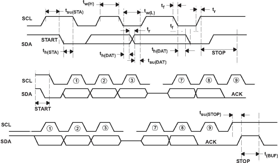 Figure 1. SMBus Communication Timing Waveforms
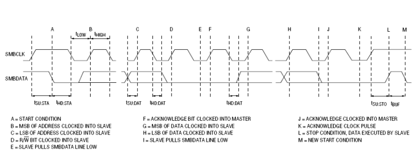 Figure 2. SMBus Writing Timing
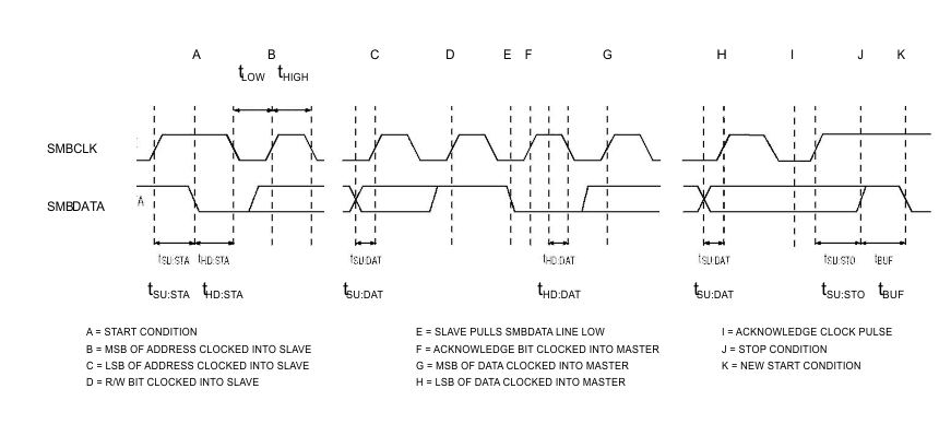 Figure 3. SMBus Read Timing
5.8 Typical Characteristics
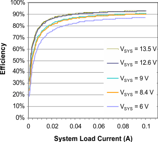
| VIN = 19.5 V |
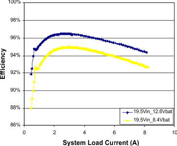
| VIN = 19.5 V |