SLUS999A November 2009 – November 2015
PRODUCTION DATA.
- 1 Features
- 2 Applications
- 3 Description
- 4 Revision History
- 5 Description (Continued)
- 6 Pin Configuration and Functions
- 7 Specifications
-
8 Detailed Description
- 8.1 Overview
- 8.2 Functional Block Diagram
- 8.3
Feature Description
- 8.3.1 Adapter Detect and Power Up
- 8.3.2 Enable and Disable Charging
- 8.3.3 Automatic Internal Soft-Start Charger Current
- 8.3.4 Switching Frequency
- 8.3.5 Converter Operation
- 8.3.6 Refresh BTST Capacitor
- 8.3.7 UCP (Charge Undercurrent): Using Sense Resistor
- 8.3.8 Cycle-By-Cycle Charge Overcurrent Protection, Using High-Side Sense-FET
- 8.3.9 Average Charge Overcurrent Protection, Using Sense Resistor
- 8.3.10 Battery Overvoltage Protection, Using Remote Sensing VFB
- 8.3.11 Battery Short Protection
- 8.3.12 Battery Trickle Charging
- 8.3.13 High Accuracy VICM Using Current Sense Amplifier (CSA)
- 8.3.14 VDDSMB Input Supply
- 8.3.15 Input Undervoltage Lockout (UVLO)
- 8.3.16 VDDP Gate Drive Regulator
- 8.3.17 Input Current Comparator Trip Detection
- 8.3.18 Open-Drain Status Outputs (ACOK, ICOUT Pins)
- 8.3.19 Thermal Shutdown Protection
- 8.3.20 Charger Timeout
- 8.3.21 Charge Termination For Li-Ion or Li-Polymer
- 8.3.22 Remote Sense
- 8.4 Device Functional Modes
- 8.5 Programming
- 8.6 Register Maps
- 9 Application and Implementation
- 10Power Supply Recommendations
- 11Layout
- 12Device and Documentation Support
- 13Mechanical, Packaging, and Orderable Information
Package Options
Mechanical Data (Package|Pins)
- RUV|34
Thermal pad, mechanical data (Package|Pins)
- RUV|34
Orderable Information
9 Application and Implementation
NOTE
Information in the following applications sections is not part of the TI component specification, and TI does not warrant its accuracy or completeness. TI’s customers are responsible for determining suitability of components for their purposes. Customers should validate and test their design implementation to confirm system functionality.
9.1 Application Information
The bq24765EVM-349 evaluation module (EVM) is a complete charger module for evaluating the bq24765. The application curves were taken using the bq24765EVM-349. Refer to the bq24765 EVM (HPA349) User's Guide, SLUU415 for EVM information.
9.2 Typical Application
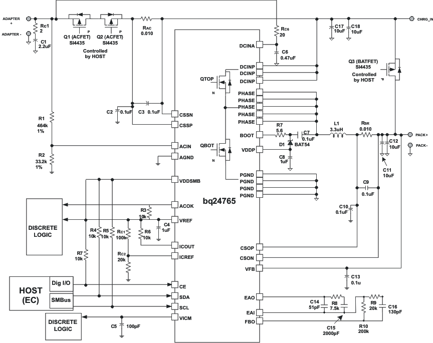
9.2.1 Design Requirements
For this design example, use the parameters listed in Table 6.
Table 6. Design Parameters
| DESIGN PARAMETER | EXAMPLE VALUE |
|---|---|
| Input Voltage(1) | 17.7 V < Adapter Voltage < 24 V |
| Input Current Limit(1) | 3.2 A for 65 W adapter |
| Battery Charge Voltage(2) | 12592 mV for 3s battery |
| Battery Charge Current(2) | 4096 mA for 3s battery |
| Battery Discharge Current(2) | 6144 mA for 3s battery |
9.2.2 Detailed Design Procedure
The parameters are configurable using the evaluation software, SLVC309. The simplified application circuit (see Figure 17) shows the minimum capacitance requirements for each pin. Inductor, capacitor, and MOSFET selection are explained in the rest of this section. Refer to the bq24765 EVM (HPA349) User's Guide, SLUU415 for the full application schematic.
Table 7. Component List For Typical System Circuit of bq24765
| PART DESIGNATOR | Qty | DESCRIPTION |
|---|---|---|
| Q1, Q2, Q6 | 3 | P-channel MOSFET, –30 V, –7.5 A, SO-8, Vishay-Siliconix, Si4835 |
| RAC, RSR | 2 | Sense Resistor, 10 mΩ, 1 W, 2010, Vishay-Dale, WSL2010R0100F |
| L1 | 1 | Inductor, 2.2 µH, 8 A, 20 mΩ, Vishay, IHLP2525CZ01-2R2 |
| 4xC2, 2xC9, 3xC13 | 9 | Capacitor, Ceramic, 10 µF, 35 V, 20%, X5R, 1206, Panasonic, ECJ-3YB1E106M |
| C1 | 1 | Capacitor, Ceramic, 2.2 µF, 25 V, 1210 |
| C3, C7, C11 | 3 | Capacitor, Ceramic, 1 µF, 25 V, 10%, X7R, 2012, TDK, C2012X7R1E105K |
| C6 | 1 | Capacitor, Ceramic, 0.47 µF, 25 V, 0805 |
| C4, C5, C10, C11, C12, C13, C15 | 7 | Capacitor, Ceramic, 0.1 µF, 50 V, 10%, X7R, 0805, Kemet, C0805C104K5RACTU |
| C8 | 1 | Capacitor, Ceramic, 100 pF, 25 V, 10%, X7R, 0805, Kemet |
| C16 | 1 | Capacitor, Ceramic, 51 pF, 25 V, 10%, X7R, 0805, Kemet |
| C17 | 1 | Capacitor, Ceramic, 2000 pF, 25 V, 10%, X7R, 0805, Kemet |
| C18 | 1 | Capacitor, Ceramic, 130 pF, 25 V, 10%, X7R, 0805, Kemet |
| RC1 | 1 | Resistor, thick film chip paralleling, 2x3.9 Ω, 25 V, 1210 |
| RC6 | 1 | Resistor, thick film chip, 20 Ω, 0805 |
| R3, R4, R5, R6, R7 | 5 | Resistor, Chip, 10 kΩ, 1/16 W, 5%, 0402 |
| R1 | 1 | Resistor, Chip, 309 kΩ, 1/16 W, 1%, 0402 |
| R2 | 1 | Resistor, Chip, 49.9 kΩ, 1/16 W, 1%, 0402 |
| R8 | 1 | Resistor, Chip, 51.1 kΩ, 1/16 W, 1%, 0402 |
| R9 | 1 | Resistor, Chip, 17.4 kΩ, 1/16 W, 1%, 0402 |
| R10 | 1 | Resistor, Chip, 7.5 kΩ, 1/16 W, 5%, 0402 |
| R11 | 1 | Resistor, Chip, 4.7 kΩ, 1/16 W, 5%, 0402 |
| R12 | 1 | Resistor, Chip, 200 kΩ, 1/16 W, 5%, 0402 |
| R13 | 1 | Resistor, Chip, 1.4 MegΩ, 1/16 W, 1%, 0402 |
9.2.3 Application Curves
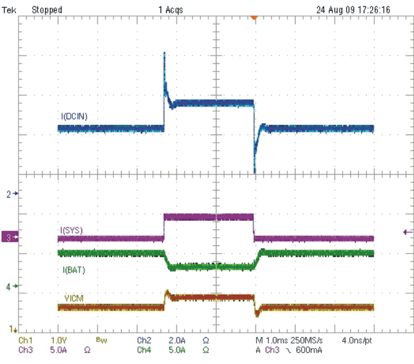 Figure 18. Transient System Load (DPM) Response: Charge Current Dropped From 4A to 2A
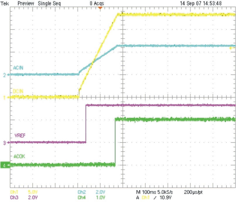 Figure 20. Charger When Adapter Inserted
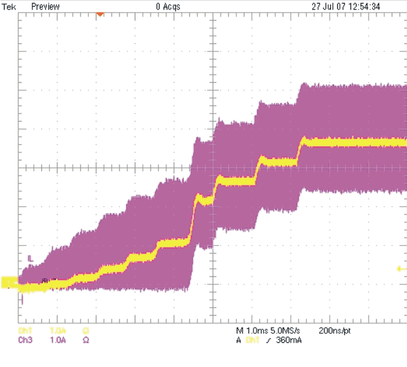 Figure 22. Inductor Current and Battery Current Soft-Start
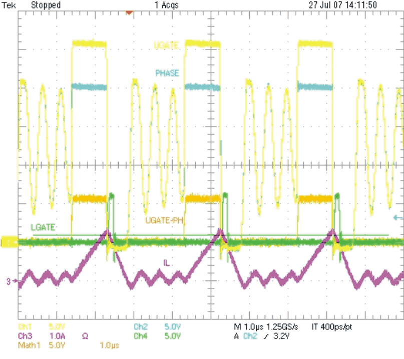 Figure 24. Discontinuous Conduction Mode (DCM) Switching Waveforms
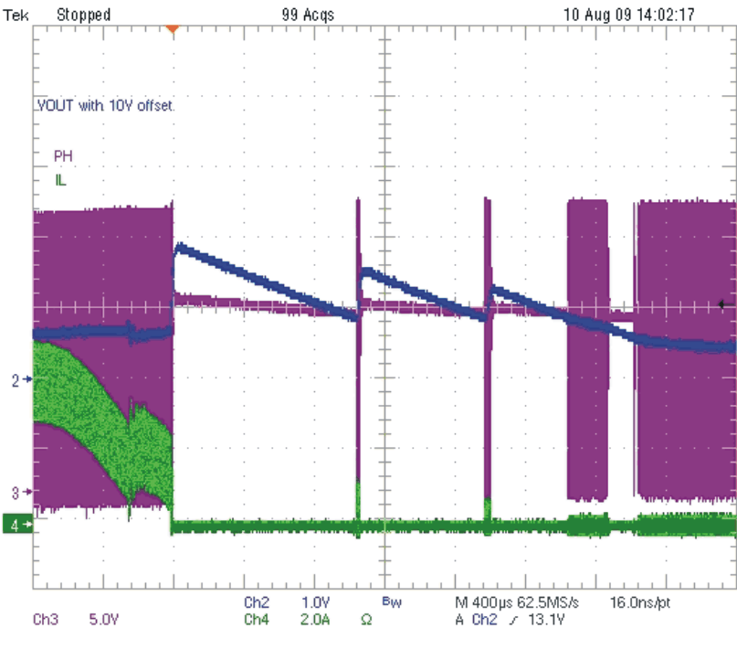 Figure 26. Battery Removal (From Constant Current Mode)
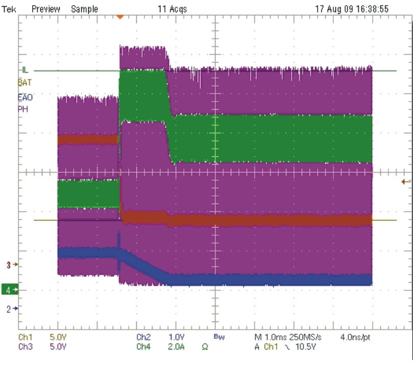 Figure 28. Power FET Overcurrent Protection
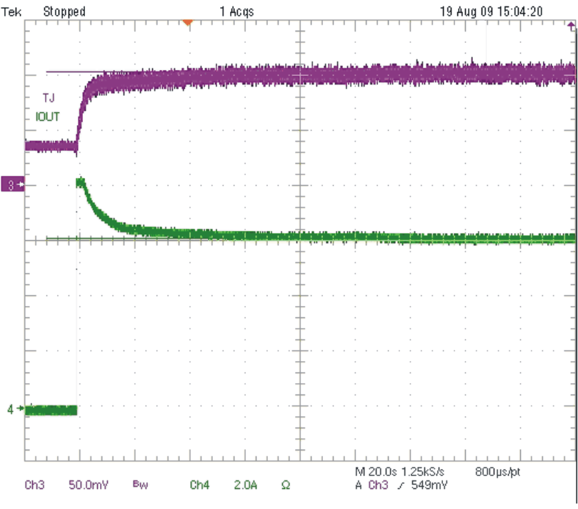 Figure 30. Thermal Regulation at TA = 40°C
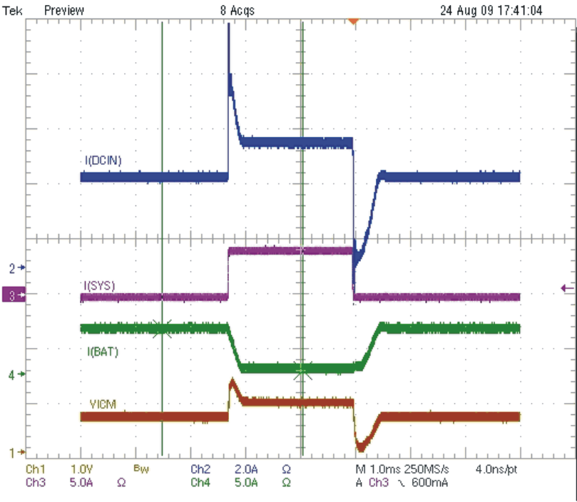 Figure 19. Transient System Load (DPM) Response: Charge Current Dropped From 4A to 0A
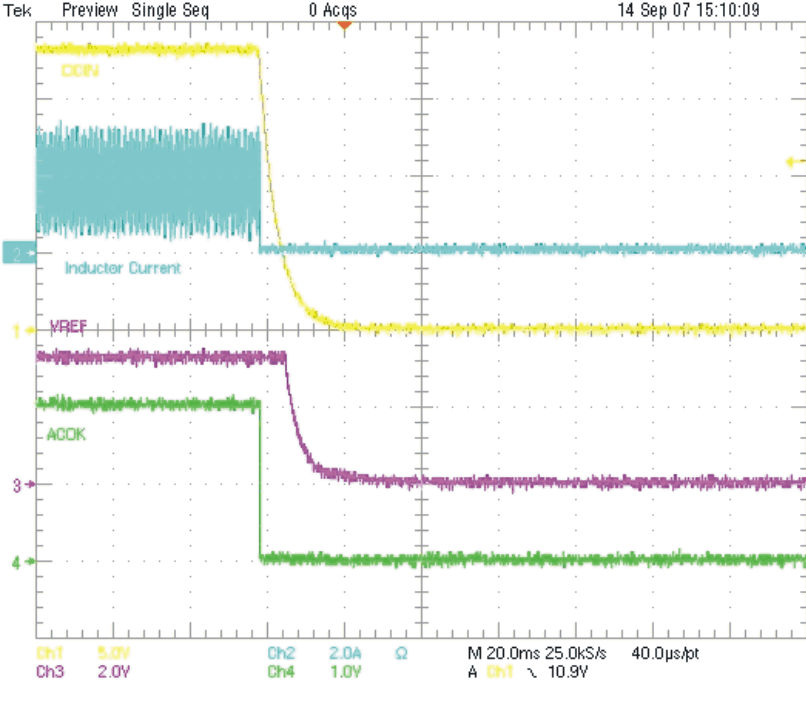 Figure 21. Charger When Adapter Removed
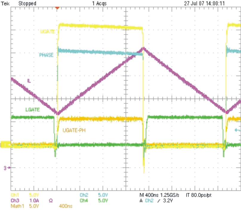 Figure 23. Continuous Conduction Mode (CCM) Switching Waveforms
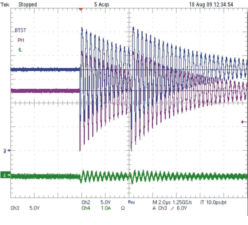 Figure 25. Near 100% Duty Cycle Bootstrap Recharge Pulse
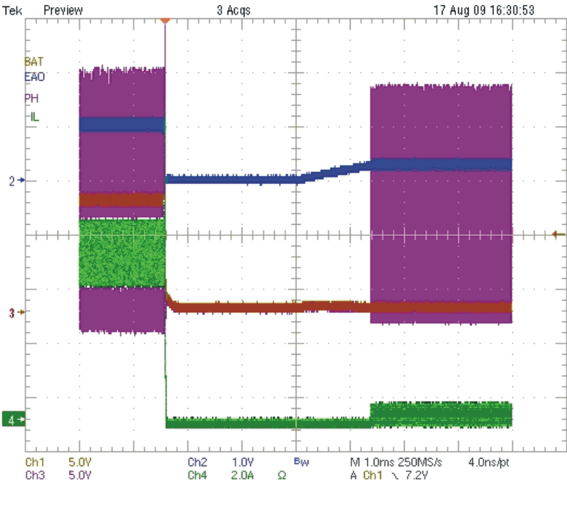 Figure 27. Battery Shorted Charger Response, Reset Charger
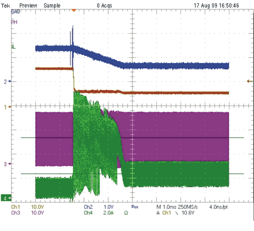 Figure 29. Charge Overcurrent Protection
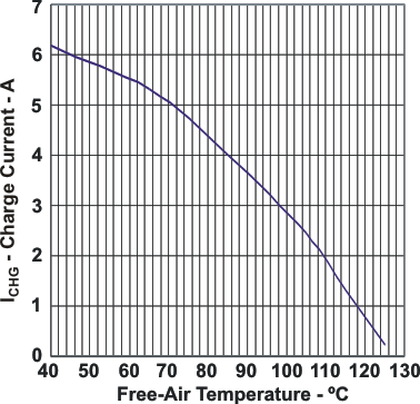 Figure 31. Charge Current vs Free-Air Temperature