SLUS999A November 2009 – November 2015
PRODUCTION DATA.
- 1 Features
- 2 Applications
- 3 Description
- 4 Revision History
- 5 Description (Continued)
- 6 Pin Configuration and Functions
- 7 Specifications
-
8 Detailed Description
- 8.1 Overview
- 8.2 Functional Block Diagram
- 8.3
Feature Description
- 8.3.1 Adapter Detect and Power Up
- 8.3.2 Enable and Disable Charging
- 8.3.3 Automatic Internal Soft-Start Charger Current
- 8.3.4 Switching Frequency
- 8.3.5 Converter Operation
- 8.3.6 Refresh BTST Capacitor
- 8.3.7 UCP (Charge Undercurrent): Using Sense Resistor
- 8.3.8 Cycle-By-Cycle Charge Overcurrent Protection, Using High-Side Sense-FET
- 8.3.9 Average Charge Overcurrent Protection, Using Sense Resistor
- 8.3.10 Battery Overvoltage Protection, Using Remote Sensing VFB
- 8.3.11 Battery Short Protection
- 8.3.12 Battery Trickle Charging
- 8.3.13 High Accuracy VICM Using Current Sense Amplifier (CSA)
- 8.3.14 VDDSMB Input Supply
- 8.3.15 Input Undervoltage Lockout (UVLO)
- 8.3.16 VDDP Gate Drive Regulator
- 8.3.17 Input Current Comparator Trip Detection
- 8.3.18 Open-Drain Status Outputs (ACOK, ICOUT Pins)
- 8.3.19 Thermal Shutdown Protection
- 8.3.20 Charger Timeout
- 8.3.21 Charge Termination For Li-Ion or Li-Polymer
- 8.3.22 Remote Sense
- 8.4 Device Functional Modes
- 8.5 Programming
- 8.6 Register Maps
- 9 Application and Implementation
- 10Power Supply Recommendations
- 11Layout
- 12Device and Documentation Support
- 13Mechanical, Packaging, and Orderable Information
Package Options
Mechanical Data (Package|Pins)
- RUV|34
Thermal pad, mechanical data (Package|Pins)
- RUV|34
Orderable Information
11 Layout
11.1 Layout Guidelines
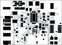
It is critical that the exposed power pad on the backside of the IC package be soldered to the PCB ground. Ensure that there are sufficient thermal vias directly under the IC, connecting to the ground plane on the other layers. The control stage and the power stage should be routed separately. At each layer, the signal ground and the power ground are connected only at the power pad.
- The AC current-sense resistor must be connected to CSSP (pin 28) and CSSN (pin 27) with a Kelvin contact. The area of this loop must be minimized. The decoupling capacitors for these pins should be placed as close to the IC as possible.
- The charge-current sense resistor must be connected to CSOP (pin 18), CSON (pin 17) with a Kelvin contact. The area of this loop must be minimized. The decoupling capacitors for these pins should be placed as close to the IC as possible.
- Decoupling capacitors for DCIN (pin 22), VREF (pin 3), and VDDP (pin 21) should be placed underneath the IC (on the bottom layer) with the interconnections to the IC as short as possible.
- Decoupling capacitors for VFB (pin 15), VICM (pin 8), and VDDSMB (pin 11) must be placed close to the corresponding IC pins with the interconnections to the IC as short as possible. Decoupling capacitors for BOOT (pin 25) must be placed close to the corresponding IC pins with the interconnections to the IC as short as possible.
- Decoupling capacitor for the charger input must be placed very close to the top switch drains and bottom source. Make the loop from input capacitor to top switch drain, top switch source, bottom switch drain, bottom switch source and return back to input capacitor power ground as small as possible.
- Make the loop from top switch source (bottom switch drain) to inductor, output capacitor, and return back to bottom switch source power ground as small as possible.
- The pcb area for top switch source and bottom switch drain should keep as small as possible to reduce EMI but keep large enough for thermal release.
- Feedback loop compensation components should be placed close to the IC EAI (pin 5), EAO (pin 4), and FBO (pin 6) with the interconnections to the IC as short as possible.
- IC UGATE (pin 24), PHASE (pin 23), and LGATE (pin 20) should use short interconnections to the MOSFET terminals to reduce parasitic inductance. LGATE (pin 20) should keep distance from PHASE (pin 23) to avoid high dv/dt noise. Make the loop from UGATE (pin 24) to top switch gate, top switch source, and return back to PHASE (pin 23) as small as possible.
11.2 Layout Example
 Figure 32. bq24765 Board Layout