SLUSCK6C May   2017  – September 2021 BQ25606

PRODUCTION DATA  

  1. Features
  2. Applications
  3. Description
  4. Revision History
  5. Description (continued)
  6. Device Comparison Table
  7. Pin Configuration and Functions
  8. Specifications
    1. 8.1 Absolute Maximum Ratings
    2. 8.2 ESD Ratings
    3. 8.3 Recommended Operating Conditions
    4. 8.4 Thermal Information
    5. 8.5 Electrical Characteristics
    6. 8.6 Timing Requirements
    7. 8.7 Typical Characteristics
  9. Detailed Description
    1. 9.1 Overview
    2. 9.2 Functional Block Diagram
    3. 9.3 Feature Description
      1. 9.3.1 Device Power Up from Battery without Input Source
      2. 9.3.2 Power Up from Input Source
        1. 9.3.2.1 Power Up REGN Regulation
        2. 9.3.2.2 Poor Source Qualification
        3. 9.3.2.3 Input Source Type Detection
          1. 9.3.2.3.1 D+/D– Detection Sets Input Current Limit in BQ25606
        4. 9.3.2.4 Input Voltage Limit Threshold Setting (VINDPM Threshold)
        5. 9.3.2.5 Converter Power Up
      3. 9.3.3 Boost Mode Operation From Battery
      4. 9.3.4 Power Path Management
        1. 9.3.4.1 Narrow VDC Architecture
        2. 9.3.4.2 Dynamic Power Management
        3. 9.3.4.3 Supplement Mode
      5. 9.3.5 Battery Charging Management
        1. 9.3.5.1 Autonomous Charging Cycle
        2. 9.3.5.2 Charging Termination
        3. 9.3.5.3 Thermistor Qualification
        4. 9.3.5.4 JEITA Guideline Compliance During Charging Mode
        5. 9.3.5.5 Boost Mode Thermistor Monitor during Battery Discharge Mode
        6. 9.3.5.6 Charging Safety Timer
      6. 9.3.6 Status Outputs ( PG, STAT)
        1. 9.3.6.1 Power Good Indicator (PG Pin)
        2. 9.3.6.2 Charging Status Indicator (STAT)
      7. 9.3.7 Protections
        1. 9.3.7.1 Input Current Limit
        2. 9.3.7.2 Voltage and Current Monitoring in Converter Operation
          1. 9.3.7.2.1 Voltage and Current Monitoring in Buck Mode
            1. 9.3.7.2.1.1 Input Overvoltage (ACOV)
            2. 9.3.7.2.1.2 System Overvoltage Protection (SYSOVP)
        3. 9.3.7.3 Voltage and Current Monitoring in Boost Mode
          1. 9.3.7.3.1 VBUS Soft Start
          2. 9.3.7.3.2 VBUS Output Protection
          3. 9.3.7.3.3 Boost Mode Overvoltage Protection
        4. 9.3.7.4 Thermal Regulation and Thermal Shutdown
          1. 9.3.7.4.1 Thermal Protection in Buck Mode
          2. 9.3.7.4.2 Thermal Protection in Boost Mode
        5. 9.3.7.5 Battery Protection
          1. 9.3.7.5.1 Battery Overvoltage Protection (BATOVP)
          2. 9.3.7.5.2 Battery Overdischarge Protection
          3. 9.3.7.5.3 System Overcurrent Protection
  10. 10Application and Implementation
    1. 10.1 Application Information
    2. 10.2 Typical Application
      1. 10.2.1 Design Requirements
      2. 10.2.2 Detailed Design Procedure
        1. 10.2.2.1 Inductor Selection
        2. 10.2.2.2 Input Capacitor
        3. 10.2.2.3 Output Capacitor
      3. 10.2.3 Application Curves
  11. 11Power Supply Recommendations
  12. 12Layout
    1. 12.1 Layout Guidelines
    2. 12.2 Layout Example
  13. 13Device and Documentation Support
    1. 13.1 Device Support
      1. 13.1.1 Third-Party Products Disclaimer
    2. 13.2 Receiving Notification of Documentation Updates
    3. 13.3 Support Resources
    4. 13.4 Trademarks
    5. 13.5 Electrostatic Discharge Caution
    6. 13.6 Glossary
  14. 14Mechanical, Packaging, and Orderable Information

Package Options

Mechanical Data (Package|Pins)
Thermal pad, mechanical data (Package|Pins)
Orderable Information

JEITA Guideline Compliance During Charging Mode

To improve the safety of charging Li-ion batteries, JEITA guideline was released on April 20, 2007. The guideline emphasized the importance of avoiding a high charge current and high charge voltage at certain low and high temperature ranges.

To initiate a charge cycle, the voltage on TS pin must be within the VT1 to VT5 thresholds. If TS voltage exceeds the T1-T5 range, the controller suspends charging and waits until the battery temperature is within the T1 to T5 range.

At cool temperature (T1-T2), the charge current is reduced to 20% of programmed fast charge current. At warm temperature (T3-T5), the charge voltage is reduced to 4.1 V. Charge termination is disabled for cool and warm conditions.

GUID-EB628AA2-B2D7-4C40-806E-7E10B026DAA8-low.gifFigure 9-2 JEITA Profile: Charging Current
GUID-3282873A-530C-4BAB-ADC5-2A26E64DFC01-low.gifFigure 9-3 JEITA Profile: Charging Voltage

Equation 1 through Equation 2 describe updates to the resistor bias network.

GUID-8F96F53D-C5F0-4DCC-88EF-87C4E579E0AA-low.gif Figure 9-4 TS Pin Resistor Network
Equation 1. GUID-789E4AC9-A11A-4AA0-AA9A-5D0D522A66F1-low.gif
Equation 2. GUID-76716FD4-5356-4270-906B-8571AEF1DBDF-low.gif

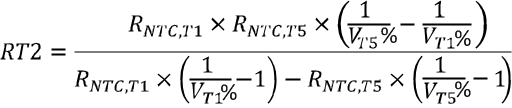
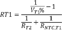
Select 0°C to 60°C range for Li-ion or Li-polymer battery:

  • RTHCOLD = 27.28 kΩ
  • RTHHOT = 3.02 kΩ
  • RT1 = 5.23 kΩ
  • RT2 = 30.9 kΩ