SLVSDU0B September 2017 – September 2019 BQ25910
PRODUCTION DATA.
- 1 Features
- 2 Applications
- 3 Description
- 4 Revision History
- 5 Pin Configuration and Functions
- 6 Specifications
-
7 Detailed Description
- 7.1 Overview
- 7.2 Functional Block Diagram
- 7.3
Feature Description
- 7.3.1 Device Power-On-Reset (POR)
- 7.3.2 Device Power Up from Battery without Input Source
- 7.3.3 Device Power Up from Input Source
- 7.3.4 Power Up REGN LDO
- 7.3.5 Poor Source Qualification
- 7.3.6 Converter Power-Up
- 7.3.7 Three-Level Buck Converter Theory of Operation
- 7.3.8 Host Mode and Default Mode
- 7.3.9 Battery Charging Management
- 7.3.10 Master Charger and Parallel Charger Interactions
- 7.3.11 Battery Charging Profile
- 7.4 Device Functional Modes
- 7.5 Programming
- 7.6
Register Maps
- 7.6.1
I2C Registers
- 7.6.1.1 Battery Voltage Regulation Limit Register (Address = 0h) [reset = AAh]
- 7.6.1.2 Charger Current Limit Register (Address = 1h) [reset = 46h]
- 7.6.1.3 Input Voltage Limit Register (Address = 2h) [reset = 04h]
- 7.6.1.4 Input Current Limit Register (Address = 3h) [reset = 13h]
- 7.6.1.5 Reserved Register (Address = 4h) [reset = 03h]
- 7.6.1.6 Charger Control 1 Register (Address = 5h) [reset = 9Dh]
- 7.6.1.7 Charger Control 2 Register (Address = 6h) [reset = 33h]
- 7.6.1.8 INT Status Register (Address = 7h) [reset = X]
- 7.6.1.9 FAULT Status Register (Address = 8h) [reset = X]
- 7.6.1.10 INT Flag Status Register (Address = 9h) [reset = 00h]
- 7.6.1.11 FAULT Flag Register (Address = Ah) [reset = 00h]
- 7.6.1.12 INT Mask Register (Address = Bh) [reset = 00h]
- 7.6.1.13 FAULT Mask Register (Address = Ch) [reset = 00h]
- 7.6.1.14 Part Information Register (Address = Dh) [reset = 0Ah]
- 7.6.1
I2C Registers
- 8 Application and Implementation
- 9 Power Supply Recommendations
- 10Layout
- 11Device and Documentation Support
- 12Mechanical, Packaging, and Orderable Information
Package Options
Refer to the PDF data sheet for device specific package drawings
Mechanical Data (Package|Pins)
- YFF|36
Thermal pad, mechanical data (Package|Pins)
Orderable Information
7.3.10 Master Charger and Parallel Charger Interactions
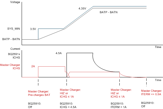
A master charger is required in the system to manage pre-charging and full termination of the battery. The BQ25910 monitors the battery voltage and compares it to VBAT_LOWV to ensure battery can safely take fast-charge current. Once the BQ25910 turns on and begins fast-charging, the host has two options: disable (HIZ) the master charger, or continue running the master charger along with the parallel charger.
For the first option, once battery voltage reaches VBAT_LOWV, the master charger maintains the BATFET on to supply system from battery (EN_HIZ = 1 on master charger), and the BQ25910 provides both the charge current and system current if required. It is recommended to select VBAT_LOWV equal to minimum system voltage in order to maintain system operation during transition. The BQ25910 will then fast-charge the battery up to VREG and continue to regulate voltage while battery current tapers down. After the BQ25910 detects termination, the host can re-enable the master charger to regulate battery voltage in CV mode down to lower termination currents.
The second mode of operation requires both chargers to stay on. In order to maximize efficiency, it is recommended to run the master charger at lower charge current than the BQ25910. For example, the master charger might be set at 1 A and the BQ25910 at 3.5 A to achieve total charge current of 4.5 A. In this mode of operation, the master charger provides mostly system current, while the BQ25910 provides mostly charge current. In this mode of operation, the BQ25910 can select VBAT_LOWV as low as the battery dictates for fast-charge, since the master charger can maintain system voltage regulation and ensure system continues to operate through the transition. After the BQ25910 detects termination, the master charger automatically continues to regulate battery voltage in CV mode down to lower termination current.
Figure 18 shows both options with charge current for each device as well as battery voltage.
 Figure 18. Master Charger and BQ25910 Handoff