SLUSB15J September   2012  – May 2021 BQ2947

PRODUCTION DATA  

  1. Features
  2. Applications
  3. Description
  4. Revision History
  5. Device Comparison Table
  6. Pin Configuration and Functions
  7. Specifications
    1. 7.1 Absolute Maximum Ratings
    2. 7.2 ESD Ratings
    3. 7.3 Recommended Operating Conditions
    4. 7.4 Thermal Information
    5. 7.5 Electrical Characteristics
    6. 7.6 Typical Characteristics
  8. Detailed Description
    1. 8.1 Overview
    2. 8.2 Functional Block Diagram
    3. 8.3 Feature Description
      1. 8.3.1 Pin Details
        1. 8.3.1.1 Input Sense Voltage, Vx
        2. 8.3.1.2 Output Drive, OUT
        3. 8.3.1.3 Supply Input, VDD
        4. 8.3.1.4 External Delay Capacitor, CD
    4. 8.4 Device Functional Modes
      1. 8.4.1 NORMAL Mode
      2. 8.4.2 OVERVOLTAGE Mode
      3. 8.4.3 Customer Test Mode
  9. Application and Implementation
    1. 9.1 Application Information
    2. 9.2 Typical Applications
      1. 9.2.1 Application Configuration for Active High
        1. 9.2.1.1 Design Requirements
        2. 9.2.1.2 Detailed Design Procedure
        3. 9.2.1.3 Application Curves
  10. 10Power Supply Recommendations
  11. 11Layout
    1. 11.1 Layout Guidelines
    2. 11.2 Layout Example
  12. 12Device and Documentation Support
    1. 12.1 Third-Party Products Disclaimer
    2. 12.2 Documentation Support
      1. 12.2.1 Related Documentation
    3. 12.3 Receiving Notification of Documentation Updates
    4. 12.4 Support Resources
    5. 12.5 Trademarks
    6. 12.6 Electrostatic Discharge Caution
    7. 12.7 Glossary
  13. 13Mechanical, Packaging, and Orderable Information

Package Options

Mechanical Data (Package|Pins)
Thermal pad, mechanical data (Package|Pins)
Orderable Information

Detailed Design Procedure

  1. Determine the number of cell in series.

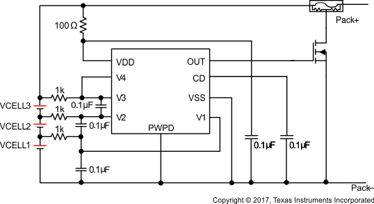
    The device supports 2-S to 4-S cell configuration. For 2S and 3S, the top unused pin(s) should be shorted as shown in Figure 9-2 and Figure 9-3.

  2. Determine the overvoltage protection delay.

    Follow the calculation example described in CD pin description. Select the right capacitor to connect to the CD pin.

  3. Follow the application schematic to connect the device. If the OUT pin is configured to open drain, an external pull up resistor should be used.
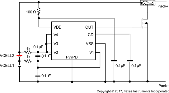
GUID-279E5559-DD19-4997-9871-ACFB14FF39EE-low.gifFigure 9-2 2-Series Cell Configuration
GUID-38388A44-4A03-4141-82D2-F9F77F7FFEDB-low.gifFigure 9-3 3-Series Cell Configuration