SLUSB96A November 2012 – December 2015
- 1 Features
- 2 Applications
- 3 Description
- 4 Revision History
- 5 Pin Configuration and Functions
- 6 Specifications
-
7 Detailed Description
- 7.1 Overview
- 7.2 Functional Block Diagram
- 7.3
Feature Description
- 7.3.1 Capacitor Selection
- 7.3.2 A6 Coil Specification
- 7.3.3 Option Select Pins
- 7.3.4 LED Modes
- 7.3.5 Parasitic Metal Object Detect (PMOD) and Foreign Object Detection (FOD)
- 7.3.6 Shut Down by Thermal Sensor or Trigger
- 7.3.7 Fault Handling and Indication
- 7.3.8 Power Transfer Start Signal
- 7.3.9 Power-On Reset
- 7.3.10 External Reset, RESET Pin
- 7.3.11 Trickle Charge and CS100
- 7.3.12 Current Monitoring Requirements
- 7.3.13 Overcurrent Protection
- 7.3.14 MSP430G2101 Low Power Supervisor
- 7.3.15 All Unused Pins
- 8 Application and Implementation
- 9 Layout
- 10Device and Documentation Support
- 11Mechanical, Packaging, and Orderable Information
Package Options
Mechanical Data (Package|Pins)
- RGZ|48
Thermal pad, mechanical data (Package|Pins)
- RGZ|48
Orderable Information
8 Application and Implementation
NOTE
Information in the following applications sections is not part of the TI component specification, and TI does not warrant its accuracy or completeness. TI’s customers are responsible for determining suitability of components for their purposes. Customers should validate and test their design implementation to confirm system functionality.
8.1 Typical Application
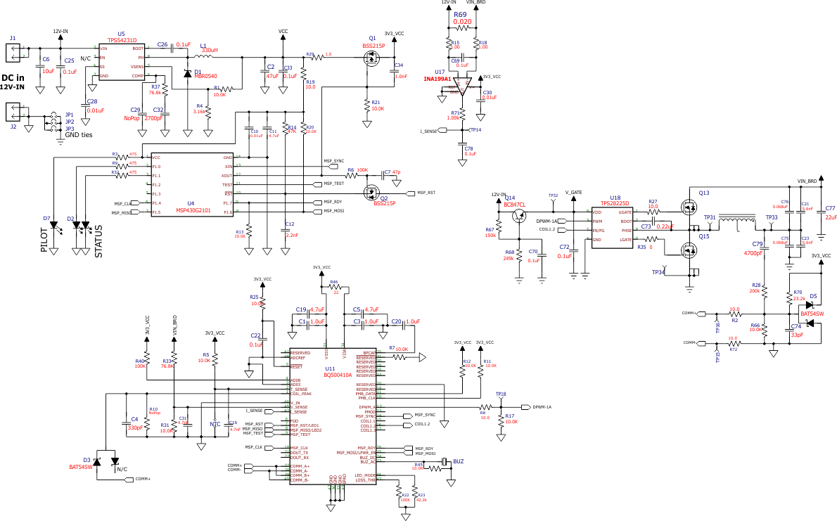
The application schematic for the transmitter with reduced standby power is shown in Figure 7.
CAUTION
Please check the bq500410A product page for the most up-to-date schematic and list of materials reference design package before starting a new project.
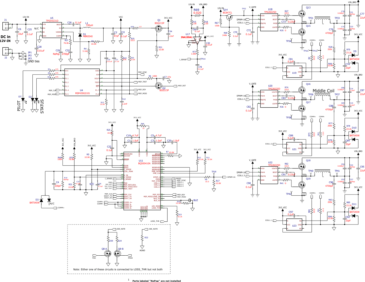
 Figure 6. bq500410A Single Coil Application Diagram
8.1.1 Detailed Design Procedure
8.1.1.1 Input Regulator
The bq500410A requires 3.3 VDC to operate. A buck regulator or a linear regulator can be used to step down from the 12-V system input. Either choice is fully WPC compatible, the decision lies in the user's requirements with respect to cost or efficiency.
Figure 6 utilizes a low-cost buck regulator, TPS54231.
8.1.1.2 Power Trains
The bq500410A drives three independent half bridges. Each half bridge drives one coil from the coil set assembly. The TPS28225 is the recommended driver device for this application. It features high-side drive capability which enables the use of N-channel MOSFETs throughout. Gate-drive supply can be derived from a primitive active voltage divider. A highly regulated supply is not required to drive MOSFET gates.
8.1.1.3 Signal Processing Components
The COMM signal used to control power transfer is derived from the coil voltage. Each coil has its own signal processing chain. The coil voltage is AC coupled and divided down to a manageable level and biased to a 1-V offset. Series connected diodes are provided for protection from any possible transients. The three signal processing chains are then multiplexed together via analog switches. Thus, the correct signal processing chain and COMM signal used to control power transfer is from the coil being driven.
8.1.1.4 Low-Power Supervisor
Power reduction is achieved by periodically disabling the bq500410A while LED and housekeeping control functions are continued by U4, the low-cost, low quiescent current micro controller MSP430G2101. When U4 is present in the circuit (which is set by a pull-up resistor on bq500410A pin 25), the bq500410A at first power-up boots the MSP430G2101 with the necessary firmware and the two chips operate in tandem. During standby operation, the bq500410A periodically issues SLEEP command, Q1 pulls the supply to the bq500410A, therefore eliminating its power consumption. Meanwhile, the MSP430G2101 maintains the LED indication and stores previous charge state during this bq500410A reset period. This bq500410A off period is set by the MSP430G2101. WPC compliance mandates the power transmitter controller, bq500410A, awakes every 400 ms to produce an analog ping and check if a valid device is present. This time constant can not be altered to further reduce power.
8.1.1.5 Disabling Low-Power Supervisor Mode
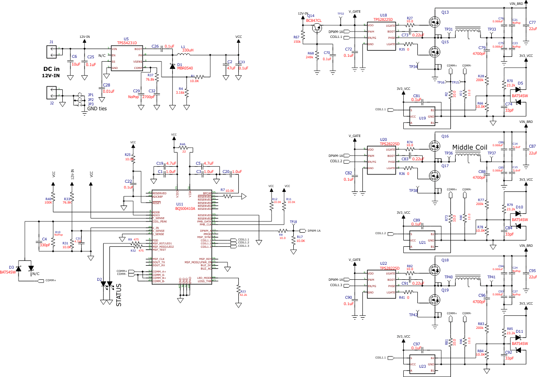
For lowest cost or if the low-power supervisor is not needed, please refer to Figure 8 for an application schematic example.
8.1.1.6 Input Power Requirements
For full wireless power system capability and WPC compliance, the AC power adapter selected for the application should have a minimum rating of 12 V at 750 mA.
8.2 System Examples
 Figure 7. bq500410A Low-Power Application Diagram
 Figure 8. bq500410A Low-Cost Application Diagram