SLUSAX0E December 2012 – April 2021 BQ7716
PRODUCTION DATA
- 1 Features
- 2 Applications
- 3 Description
- 4 Revision History
- 5 Device Comparison Table
- 6 Pin Configuration and Functions
- 7 Specifications
- 8 Detailed Description
- 9 Application and Implementation
- 10Power Supply Recommendations
- 11Layout
- 12Device and Documentation Support
- 13Mechanical, Packaging, and Orderable Information
Package Options
Mechanical Data (Package|Pins)
- DPJ|8
Thermal pad, mechanical data (Package|Pins)
Orderable Information
8.3 Feature Description
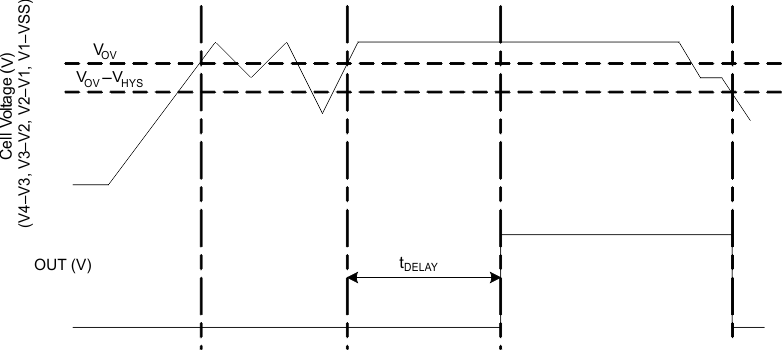
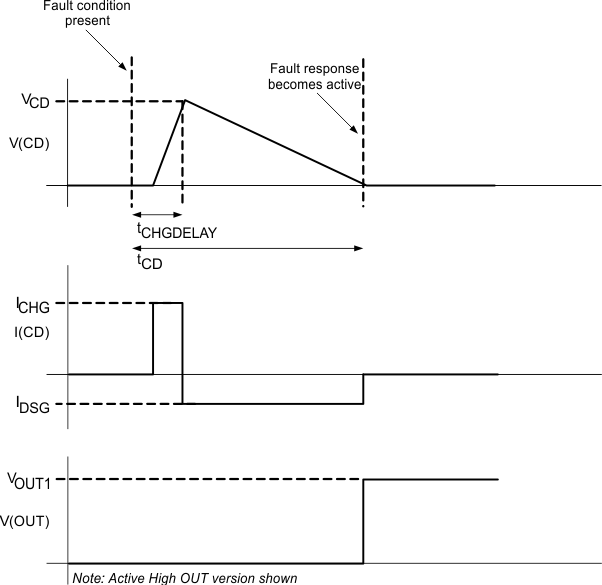
In the BQ7716xy device, each cell is monitored independently. Overvoltage is detected by comparing the actual cell voltage to a protection voltage reference, VOV. If any cell voltage exceeds the programmed OV value, a timer circuit is activated. This timer circuit charges the CD pin to a nominal value, then slowly discharges it with a fixed current back down to VSS. When the CD pin falls below a nominal threshold near VSS, the OUT terminal goes from inactive to active state. Additionally, a timeout detection circuit checks to ensure that the CD pin successfully begins charging to above VSS and subsequently drops back down to VSS, and if a timeout error is detected in either direction, it will similarly trigger the OUT pin to become active. See Figure 8-1 for reference.
For an NCH Open Drain Active Low configuration, the OUT pin pulls down to VSS when active (OV present), and is high impedance when inactive (no OV).
 Figure 8-1 Timing for Overvoltage Sensing
Figure 8-2 shows an overview of the behavior of the CD pin during an OV sequence.
 Figure 8-2 CD Pin Mechanism