SCAS882E June   2009  – October 2016 CDCE62002

PRODUCTION DATA.  

  1. Features
  2. Applications
  3. Description
  4. Revision History
  5. Description (continued)
  6. Pin Configuration and Functions
  7. Specifications
    1. 7.1 Absolute Maximum Ratings
    2. 7.2 Thermal Information
    3. 7.3 Electrical Characteristics
    4. 7.4 Timing Requirements
    5. 7.5 SPI Bus Timing Characteristics
    6. 7.6 Typical Characteristics
  8. Parameter Measurement Information
  9. Detailed Description
    1. 9.1 Overview
    2. 9.2 Functional Block Diagrams
      1. 9.2.1 Interface and Control Block
      2. 9.2.2 Input Block
      3. 9.2.3 Output Block
      4. 9.2.4 Synthesizer Block
      5. 9.2.5 Computing the Output Frequency
    3. 9.3 Feature Description
      1. 9.3.1 Phase Noise Analysis
      2. 9.3.2 Output-to-Output Isolationthe OUTPUT TO OUTPUT ISOLATION section
      3. 9.3.3 Device Control
      4. 9.3.4 External Control Pins
        1. 9.3.4.1 Factory Default Programming
      5. 9.3.5 Input Block
        1. 9.3.5.1 Reference Input Buffer
        2. 9.3.5.2 Smart Multiplexer Dividers
        3. 9.3.5.3 Auxiliary Input Port
        4. 9.3.5.4 Output Block
        5. 9.3.5.5 Synthesizer Block
        6. 9.3.5.6 Input Divider
        7. 9.3.5.7 Feedback and Feedback Bypass Divider
          1. 9.3.5.7.1 VCO Select
          2. 9.3.5.7.2 Prescaler
          3. 9.3.5.7.3 Loop Filter
        8. 9.3.5.8 Internal Loop Filter Component Configuration
      6. 9.3.6 Lock Detect
      7. 9.3.7 Crystal Input Interface
      8. 9.3.8 VCO Calibration
      9. 9.3.9 Start-Up Time Estimation
    4. 9.4 Device Functional Modes
      1. 9.4.1 Clock Generator
      2. 9.4.2 SERDES Start-Up and Clock Cleaner
      3. 9.4.3 Clocking ADCS With the CDCE62002
    5. 9.5 Programming
      1. 9.5.1 Interface and Control Block
        1. 9.5.1.1 SPI (Serial Peripheral Interface)
        2. 9.5.1.2 SPI Interface Master
        3. 9.5.1.3 SPI Consecutive Read/Write Cycles to the CDCE62002
        4. 9.5.1.4 Writing to the CDCE62002
        5. 9.5.1.5 Reading from the CDCE62002
        6. 9.5.1.6 Writing to EEPROM
        7. 9.5.1.7 CDCE62002 SPI Command Structure
      2. 9.5.2 Device Configuration
    6. 9.6 Register Maps
      1. 9.6.1 Device Registers: Register 0 Address 0x00
      2. 9.6.2 Device Registers: Register 1 Address 0x01
      3. 9.6.3 Device Registers: Register 2 Address 0x02
  10. 10Power Supply Recommendations
  11. 11Layout
    1. 11.1 Layout Guidelines
    2. 11.2 Layout Example
  12. 12Device and Documentation Support
    1. 12.1 Receiving Notification of Documentation Updates
    2. 12.2 Community Resources
    3. 12.3 Trademarks
    4. 12.4 Electrostatic Discharge Caution
    5. 12.5 Glossary
  13. 13Mechanical, Packaging, and Orderable Information
    1. 13.1 Package

Package Options

Mechanical Data (Package|Pins)
Thermal pad, mechanical data (Package|Pins)
Orderable Information

11 Layout

11.1 Layout Guidelines

Figure 38 shows a conceptual layout focusing on power supply bypass capacitor placement. If the capacitors are mounted on the back side, 0402 components can be employed; however, soldering to the thermal dissipation pad can be difficult. If the capacitors are mounted on the component side, 0201 components must be used to facilitate signal routing. In either case, the connections between the capacitor and the power supply terminal on the device must be kept as short as possible.

11.2 Layout Example
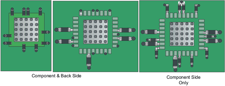
CDCE62002 ps_bypass_cas882.gif Figure 38. CDCE62002 Power Supply Bypassing