SCAS918D June 2013 – February 2024 CDCE913-Q1 , CDCEL913-Q1
PRODUCTION DATA
- 1
- 1 Features
- 2 Applications
- 3 Description
- 4 Device Comparison
- 5 Pin Configuration and Functions
- 6 Specifications
- 7 Parameter Measurement Information
- 8 Detailed Description
- 9 Application and Implementation
- 10Register Maps
- 11Device and Documentation Support
- 12Revision History
- 13Mechanical, Packaging, and Orderable Information
Package Options
Mechanical Data (Package|Pins)
- PW|14
Thermal pad, mechanical data (Package|Pins)
- PW|14
Orderable Information
9.2.2.2 PLL Frequency Planning
At a given input frequency (fIN), use Equation 1 to calculate the output frequency (fOUT) of the CDCE913-Q1 or CDCEL913-Q1 device.
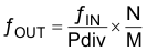
where
- M (1 to 511) and N (1 to 4095) are the multiplier or divider values of the PLL
- Pdiv (1 to 127) is the output divider
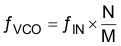
Use Equation 2 to calculate the target VCO frequency (ƒVCO) of each PLL.
The PLL internally operates as fractional divider and requires the following multiplier or divider settings:
- N
- P = 4 – int(log2N / M); if P < 0 then P = 0
- Q = int(N' / M)
- R = N′ – M × Q
where
- int(X) = integer portion of X
- N′ = N × 2P
- N ≥ M
80 MHz ≤ ƒVCO ≤ 230 MHz
16 ≤ Q ≤ 63 µs
0 ≤ P ≤ 4 µs
0 ≤ R ≤ 51 µs
| Example: | |||
| for ƒIN = 27 MHz; M = 1; N = 4; Pdiv = 2 | for ƒIN = 27 MHz; M = 2; N = 11; Pdiv = 2 | ||
| → | fOUT = 54 MHz | → | fOUT = 74.25 MHz |
| → | fVCO = 108 MHz | → | fVCO = 148.50 MHz |
| → | P = 4 – int(log24) = 4 – 2 = 2 | → | P = 4 – int(log25.5) = 4 – 2 = 2 |
| → | N' = 4 × 22 = 16 | → | N' = 11 × 22 = 44 |
| → | Q = int(16) = 16 | → | Q = int(22) = 22 |
| → | R = 16 – 16 = 0 | → | R = 44 – 44 = 0 |
The values for P, Q, R, and N' are automatically calculated when using TI Pro-Clock™ software.
The frequency of CLK1 shown in the application diagram can be obtained by passing the input frequency of the VCXO directly to output 1. The CLK2 frequency can be achieved by using the PLL constants derived in the first example. The value of CLK3 requires the same PLL constants as CLK2, but Pdiv3 is set to 1 instead of 2 to yield a frequency of 108 MHz.