SLLS781D February   2007  – November 2014 CDCL1810

PRODUCTION DATA.  

  1. Features
  2. Applications
  3. Description
  4. Functional Block Diagram
  5. Revision History
  6. Device Comparison Table
  7. Pin Configuration and Functions
  8. Specifications
    1. 8.1 Absolute Maximum Ratings
    2. 8.2 Handling Ratings
    3. 8.3 Recommended Operating Conditions
    4. 8.4 Added Thermal Information tableThermal Information
    5. 8.5 DC Electrical Characteristics
    6. 8.6 AC Electrical Characteristics
    7. 8.7 AC Electrical Characteristics for The SDA/SCL Interface
    8. 8.8 Typical Characteristics
  9. Detailed Description
    1. 9.1 Overview
    2. 9.2 Functional Block Diagrams
    3. 9.3 Feature Description
      1. 9.3.1 Output Enable/Disable
    4. 9.4 SDA/SCL Connections Recommendations
    5. 9.5 Device Functional Modes
    6. 9.6 Programming
      1. 9.6.1 SDA/SCL Interface
        1. 9.6.1.1 SDA/SCL Bus Slave Device Address
        2. 9.6.1.2 Command Code Definition
        3. 9.6.1.3 SDA/SCL Programming Sequence
    7. 9.7 SDA/SCL Bus Configuration Command Bitmap
      1. 9.7.1 Byte 0:
      2. 9.7.2 Byte 1:
      3. 9.7.3 Byte 2:
      4. 9.7.4 Byte 3:
      5. 9.7.5 Byte 4:
      6. 9.7.6 Byte 5:
      7. 9.7.7 Byte 6:
  10. 10Application and Implementation
    1. 10.1 Application Information
      1. 10.1.1 Clock Distribution for Multiple TI Keystone DSPs
        1. 10.1.1.1 Design Requirements
        2. 10.1.1.2 Detailed Design Procedure
        3. 10.1.1.3 Application Curves
  11. 11Power Supply Recommendations
  12. 12Layout
    1. 12.1 Layout Guidelines
    2. 12.2 Layout Example
  13. 13Device and Documentation Support
    1. 13.1 Trademarks
    2. 13.2 Electrostatic Discharge Caution
    3. 13.3 Glossary
  14. 14Mechanical, Packaging, and Orderable Information

Package Options

Mechanical Data (Package|Pins)
Thermal pad, mechanical data (Package|Pins)
Orderable Information

7 Pin Configuration and Functions

48-PIN VQFN
Package RGZ
(Top View)
pinout_lls781.gif
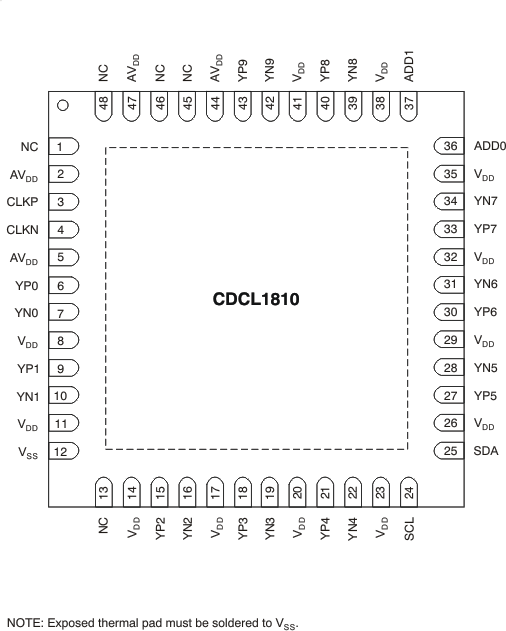
The CDCL1810 is available in a 48-pin VQFN (RGZ) package with a pin pitch of 0.5 mm. The exposed thermal pad serves both thermal and electrical grounding purposes.

The device must be soldered to ground (VSS) using as many ground vias as possible. The device performance will be severely impacted if the exposed thermal pad is not grounded appropriately.

Pin Functions

PIN TYPE DESCRIPTION
NAME PIN NO.
VDD 8, 11, 14, 17, 20, 23, 26, 29, 32, 35, 38, 41 Power 1.8-V digital power supply.
AVDD 2, 5, 44, 47 Power 1.8-V analog power supply.
VSS Exposed thermal pad and pin 12 Power Ground reference.
NC 1, 13, 45, 46, 48 I Not connected; leave open.
CLKP, CLKN 3, 4 I Differential LVDS input. Single-ended 1.8-V input can be dc-coupled to pin 3 with pin 4 either tied to pin 3 (recommended) or left open.
YP0, YN0
YP1, YN1
YP2, YN2
YP3, YN3
YP4, YN4
YP5, YN5
YP6, YN6
YP7, YN7
YP8, YN8
YP9, YN9
6, 7
9, 10
15, 16
18, 19
21, 22
27, 28
30, 31
33, 34
40, 39
43, 42
O 10 differential CML outputs.
SCL 24 I SCL serial clock pin. SCL tolerated 1.8V on the input only. Open drain. Always connect to a pull-up resistor.
SDA 25 I/O SDA bidirectional serial data pin. SDA tolerates 1.8 V on the input only.Open drain. Always connect to a pull-up resistor.
ADD1, ADD0 37, 36 I Configurable least significant bits (ADD[1:0]) of the SDA/SCL device address. The fixed most significant bits (ADD[6:2]) of the 7-bit device address are 11010.