SCAS841D February 2007 – December 2016 CDCLVD110A
PRODUCTION DATA.
- 1 Features
- 2 Applications
- 3 Description
- 4 Revision History
- 5 Pin Configuration and Functions
- 6 Specifications
- 7 Parameter Measurement Information
- 8 Detailed Description
- 9 Application and Implementation
- 10Power Supply Recommendations
- 11Layout
- 12Device and Documentation Support
- 13Mechanical, Packaging, and Orderable Information
Package Options
Mechanical Data (Package|Pins)
Thermal pad, mechanical data (Package|Pins)
- RHB|32
Orderable Information
8 Detailed Description
8.1 Overview
The CDCLVD110A LVDS drivers use CMOS transistors to control the output current. Therefore, proper biasing and termination are required to ensure correct operation of the device and to maximize signal integrity. The proper LVDS termination for signal integrity over two 50-Ω lines is 100 Ω between the outputs on the receiver end. Either DC-coupled termination or AC-coupled termination can be used for LVDS outputs. TI recommends placing a termination resistor close to the receiver. If the receiver is internally biased to a voltage different than the output common-mode voltage of the CDCLVD110A, AC-coupling must be used. If the LVDS receiver has internal 100-Ω termination, external termination must be omitted.
8.2 Functional Block Diagram

8.3 Feature Description
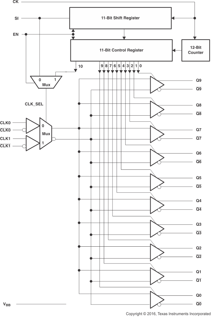
The two inputs of the CDCLVD110A are internally muxed together and can be selected trough the control pin. Unused inputs and outputs can be left floating to reduce overall component cost. Both AC- and DC-coupling schemes can be used with the CDCLVD110A to provide greater system flexibility.
8.4 Device Functional Modes
Table 1 lists the functional modes of the device.
Table 1. Truth Table For Control Logic
| CK | EN | SI | CLK0 | CLK0 | CLK1 | CLK1 | Q(0-9) | Q(0-9) |
|---|---|---|---|---|---|---|---|---|
| L | L | L | L | H | X | X | L | H |
| L | L | L | H | L | X | X | H | L |
| L | L | L | Open | Open | X | X | L | H |
| L | L | H | X | X | L | H | L | H |
| L | L | H | X | X | H | L | H | L |
| L | L | H | X | X | Open | Open | L | H |
| All outputs enabled | X = Don't care | |||||||
8.4.1 Fail-Safe Information
For VDD = 0 V (power-down mode), the CDCLVD110A has fail-safe input and output pins. In power-on mode, fail-safe biasing at input pins can be accomplished with a 10-kΩ pullup resistor from CLK0 or CLK1 to VDD and a 10-kΩ pulldown resistor from CLK0 or CLK1 to GND.
8.4.2 LVDS Receiver Input Termination
The LVDS receiver inputs require 100-Ω termination resistors placed as close as possible across the input pins.
8.4.3 Input Termination
The CDCLVD110A inputs can be interfaced with LVDS, LVPECL, or LVCMOS drivers.
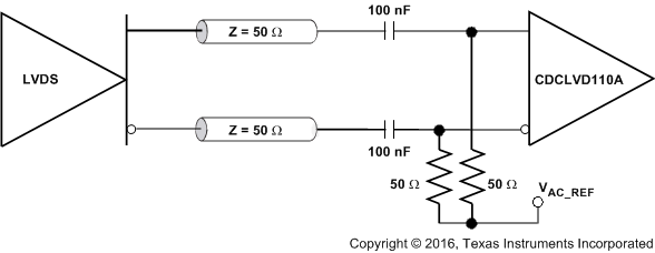
LVDS drivers can be connected to CDCLVD110A inputs with AC- and DC-coupling as shown in Figure 8 and Figure 9 (respectively).
 Figure 8. LVDS Clock Driver Connected to CDCLVD110A Input (AC-Coupled)
 Figure 9. LVDS Clock Driver Connected to CDCLVD110A Input (DC-Coupled)
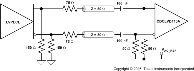
Figure 10 shows how to connect LVPECL inputs to the CDCLVD110A. The series resistors are required to reduce the LVPECL signal swing if the signal swing is >1.6 VPP.
 Figure 10. LVPECL Clock Driver Connected to CDCLVD110A Input
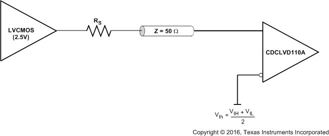
Figure 11 illustrates how to couple a 2.5-V LVCMOS clock input to the CDCLVD110A directly. The series resistance, RS, must be placed close to the LVCMOS driver if required. 3.3-V LVCMOS clock input swing must be limited to VIH ≤ VCC.
 Figure 11. 2.5-V LVCMOS Clock Driver Connected to CDCLVD110A Input
For unused input, TI recommends grounding both input pins (INP, INN) using 1-kΩ resistors.
8.4.4 LVDS Output Termination
Unused outputs can be left open without connecting any trace to the output pins.
The CDCLVD110A can be connected to LVDS receiver inputs with DC- and AC-coupling as shown in Figure 12 and Figure 13 (respectively).
 Figure 12. Output DC Termination
 Figure 13. Output AC Termination (With the Receiver Internally Biased)
8.4.5 Control Inputs Termination
No external termination is required. The CK control input has an internal 120-kΩ pullup resistor, while the SI– and EN–control inputs each have an internal 120-kΩ pulldown resistor. If the control pins are left open per the default, all outputs are enabled, CLK0 or CLK0 is selected, and the control register is disabled.
8.5 Programming
8.5.1 Specification of Control Register
The CDCLVD110A has an 11-bit, serial-in shift register and an 11-bit control register. The control Register enables or disables each output clock, and selects either CLK0 or CLK1 as the input clock. The CDCLVD110A has two modes of operation: Programmable Mode (EN = 1) and Standard Mode (EN = 0).
8.5.1.1 Programmable Mode (EN = 1)
The shift register uses a serial input (SI) and a clock input (CK). Once the shift register is loaded with 11 clock pulses, the 12th clock pulse loads the control register. The first bit (bit 0) on SI enables the Q9-Q9 output pair, and the 10th bit (bit 9) enables the Q0-Q0 pair. The 11th bit (bit 10) on SI selects either CLK0 or CLK1 as the input clock; a bit value of 0 selects CLK0, whereas a bit value of 1 selects CLK1. To restart the control register configuration, a reset of the state machine must be done with a clock pulse on CK (shift register clock input) and EN set to low. The control register can be configured only once after each reset.
8.5.1.2 Standard Mode (EN = 0)
In this mode, the CDCLVD110A is not programmable and all the clock outputs are enabled. The clock input (CLK0 or CLK1) is selected with the SI pin, as is shown in the table entitled control register.
8.6 Register Maps
Table 2. State-Machine Inputs
| EN | SI | CK | OUTPUT |
|---|---|---|---|
| L | L | X | All outputs enabled, CLK0 selected, control register disabled, default state |
| L | H | X | All outputs enabled, CLK1 selected, control register disabled |
| H | L | ↑ | First stage stores L, other stage stores data of previous stage |
| H | H | First stage stores H, other stage stores data of previous stage | |
| L | X | Reset of state machine, shift and control registers |
Table 3. Control Registers
| BIT 10 | BITS [0-9] | QN[0-9] |
|---|---|---|
| L | H | CLK0 |
| H | H | CLK1 |
| X | L | Outputs disabled |
8.6.1 Register Descriptions
Table 1. Serial Input (SI) Sequence
| BIT 10 | BIT 9 | BIT 8 | BIT 7 | BIT 6 | BIT 5 | BIT 4 | BIT 3 | BIT 2 | BIT 1 | BIT 0 |
|---|---|---|---|---|---|---|---|---|---|---|
| CLK_SEL | Q0 | Q1 | Q2 | Q3 | Q4 | Q5 | Q6 | Q7 | Q8 | Q9 |