SCAS871H February 2009 – January 2016 CDCM61004
PRODUCTION DATA.
- 1 Features
- 2 Applications
- 3 Description
- 4 Revision History
- 5 Description (Continued)
- 6 Pin Configuration and Functions
-
7 Specifications
- 7.1 Absolute Maximum Ratings
- 7.2 ESD Ratings
- 7.3 Recommended Operating Conditions
- 7.4 Thermal Information
- 7.5 Electrical Characteristics
- 7.6 Typical Output Phase Noise CharacteristicsCorrected units for tRJIT (RMS phase jitter); changed to fs, RMS from ps, RMS
- 7.7 Typical Output Jitter Characteristics
- 7.8 Crystal Characteristics
- 7.9 Dissipation Ratings
- 7.10 Typical Characteristics
- 8 Parameter Measurement Information
-
9 Detailed Description
- 9.1 Overview
- 9.2 Functional Block Diagram
- 9.3
Feature Description
- 9.3.1 Phase-Locked Loop (PLL)
- 9.3.2 Configuring the PLL
- 9.3.3 Crystal Input Interface
- 9.3.4 Phase Frequency Detector (PFD)
- 9.3.5 Charge Pump (CP)
- 9.3.6 On-Chip PLL Loop Filter
- 9.3.7 Prescaler Divider and Feedback Divider
- 9.3.8 On-Chip VCO
- 9.3.9 LVCMOS Input Interface
- 9.3.10 Output Divider
- 9.3.11 Output Buffer
- 9.4 Device Functional Modes
- 10Application and Implementation
- 11Power Supply Recommendations
- 12Layout
- 13Device and Documentation Support
- 14Mechanical, Packaging, and Orderable Information
Package Options
Mechanical Data (Package|Pins)
- RHB|32
Thermal pad, mechanical data (Package|Pins)
- RHB|32
Orderable Information
10 Application and Implementation
NOTE
Information in the following applications sections is not part of the TI component specification, and TI does not warrant its accuracy or completeness. TI’s customers are responsible for determining suitability of components for their purposes. Customers should validate and test their design implementation to confirm system functionality.
10.1 Application Information
10.1.1 Start-Up Time Estimation
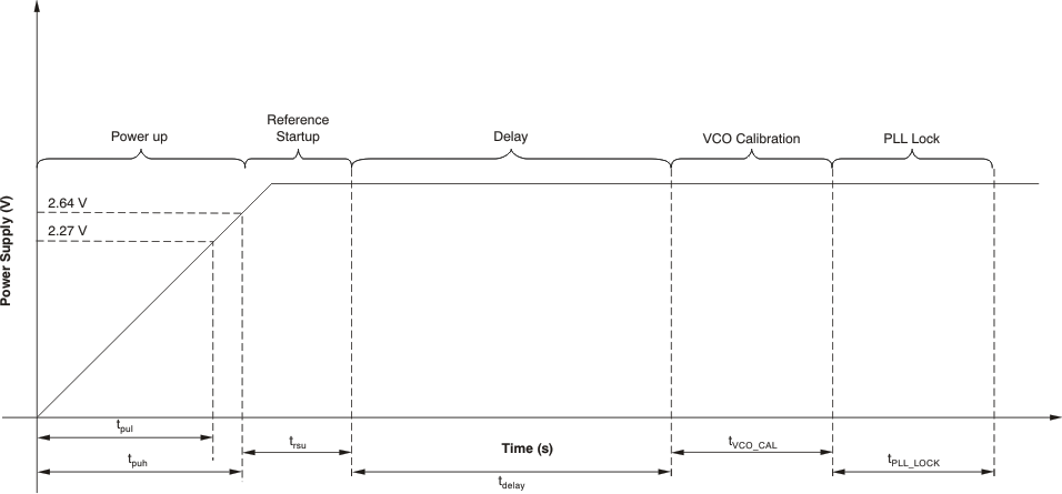
The CDCM61004 start-up time can be estimated based on the parameters defined in Table 9 and graphically shown in Figure 16.
Table 9. Start-Up Time Dependencies
| PARAMETER | DEFINITION | DESCRIPTION | FORMULA/METHOD OF DETERMINATION |
|---|---|---|---|
| tREF | Reference clock period | The reciprocal of the applied reference frequency in seconds. |  |
| tpul | Power-up time (low limit) | Power-supply rise time to low limit of Power On Reset (POR) trip point | Time required for power supply to ramp to 2.27 V |
| tpuh | Power-up time (high limit) | Power supply rise time to high limit of POR trip point | Time required for power supply to ramp to 2.64 V |
| trsu | Reference start-up time | After POR releases, the Colpits oscillator is enabled. This start-up time is required for the oscillator to generate the requisite signal levels for the delay block to be clocked by the reference input. | 500 μs best-case and 800 μs worst-case |
| tdelay | Delay time | Internal delay time generated from the reference clock. This delay provides time for the reference oscillator to stabilize. | tdelay= 16384 × tref |
| tVCO_CAL | VCO calibration time | VCO Calibration Time generated from the reference clock. This process selects the operating point for the VCO based on the PLL settings. | tVCO_CAL= 550 × tref |
| tPLL_LOCK | PLL lock time | Time required for PLL to lock within ±10 ppm of fREF | Based on the 400-kHz loop bandwidth, the PLL settles in 5τ or 12.5 μs. |
 Figure 16. Start-up Time Dependencies
The CDCM61004 start-up time limits, tMAX and tMIN, can be calculated as follows in Equation 3 and Equation 4:
10.1.2 Output Termination
The CDCM61004 is a 3.3-V clock driver with the following output options: LVPECL, LVDS, or LVCMOS.
10.1.3 LVPECL Termination
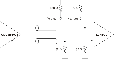
The CDCM61004 is an open emitter for LVPECL outputs. Therefore, proper biasing and termination are required to ensure correct operation of the device and to minimize signal integrity. The proper termination for LVPECL is 50 Ω to (VCC–2) V, but this DC voltage is not readily available on most PCBs. Thus, a Thevenin equivalent circuit is worked out for the LVPECL termination in both direct-coupled (DC) and ac-coupled (AC) cases, as shown in Figure 17 and Figure 18. TI recommends placing all resistive components close to either the driver end or the receiver end. If the supply voltage of the driver and receiver are different, ac-coupling is required.
 Figure 18. LVPECL Output AC Termination
10.1.4 LVDS Termination
The proper LVDS termination for signal integrity over two 50-Ω lines is 100 Ω between the outputs on the receiver end. Either direct-coupled termination or ac-coupled termination can be used for LVDS outputs, as shown in Figure 19 and Figure 20. TI recommends placing all resistive components close to either the driver end or the receiver end. If the supply voltage of the driver and the receiver are different, ac-coupling is required.
 Figure 19. LVDS Output DC Termination
 Figure 20. LVDS Output AC Termination
10.1.5 LVCMOS Termination
Series termination is a common technique used to maintain the signal integrity for LVCMOS drivers, if connected to a receiver with a high-impedance input with a pullup or a pulldown resistor. For series termination, a series resistor (RS) is placed close to the driver, as shown in Figure 21. The sum of the driver impedance and RS should be close to the transmission line impedance, which is usually 50 Ω. Because the LVCMOS driver in the CDCM61004 has an impedance of 30 Ω, RS is recommended to be 22 Ω to maintain proper signal integrity.
 Figure 21. LVCMOS Output Termination
10.1.6 Interfacing Between LVPECL and HCSL
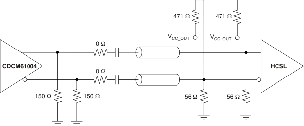
Because the LVPECL common-mode voltage is different from the HCSL common-mode voltage, ac-coupled termination is used. The 150-Ω resistor ensures proper biasing of the CDCM61004 LVPECL output stage, while the 471-Ω and 56-Ω resistor network biases the HCSL receiver input stage, as shown in Figure 22.
10.2 Typical Application
 Figure 23. Ethernet Switch
10.2.1 Design Requirements
Consider a typical wired communications application, like a top-of-rack switch, which needs to clock 1-Gbps or 3.125-Gbps Ethernet PHYs. For such asynchronous systems, the reference input can be a crystal. In such systems, the clocks are expected to be available upon power up without the need for any device-level programming. An example of clock input and output requirements is shown below:
- Clock Input:
- 25-MHz crystal
- Clock Outputs:
- 2× 156.25 MHz clock for uplink 3.125 Gbps, LVPECL
- 2× 156.25 MHz clock for downlink 3.125 Gbps, LVPECL
The section below describes the detailed design procedure to generate the required output frequencies for the above scenario using CDCM61004.
10.2.2 Detailed Design Procedure
Design of all aspects of the CDCM61004 is quite involved and software support is available to assist in part selection and phase noise simulation. This design procedure will give a quick outline of the process.
- Device Selection
- The first step is to calculate the VCO frequency given the required output frequency. The device must be able to produce the VCO frequency that can be divided down to the required output frequency.
- The WEBENCH Clock Architect Tool from TI will aid in the selection of the right device that meets the customer's output frequencies and format requirements.
- Device Configuration
- The WEBENCH Clock Architect Tool attempts to maximize the phase detector frequency, use smallest dividers, and maximizes PLL bandwidth.
10.2.2.1 Device Selection
Use the WEBENCH Clock Architect Tool. Enter the required frequencies and formats into the tool. To use this device, find a solution using the CDCM61004.
10.2.2.1.1 Calculation Using LCM
In this example, the valid VCO frequency for CDCM61004 is 1.875 GHz.
10.2.2.2 Device Configuration
For this example, when using the WEBENCH Clock Architect Tool, the reference would have been manually entered as 25 MHz according to input frequency requirements. Enter the desired output frequencies and click on Generate Solutions. Select CDCM61004 from the solution list.
From the simulation page of the WEBENCH Clock Architect Tool, it can be seen that to maximize phase detector frequencies, the N divider is set to 25 and prescaler divider is set to 3. This results in a VCO frequency of
1.875
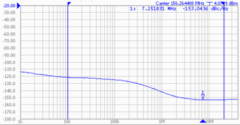
GHz. The output divider is set to 4. At this point the design meets all input and output frequency requirements and it is possible to design a loop filter for system and simulate performance on the clock outputs. Figure 24 shows the typical phase noise plot of the 156.25 MHz LVPECL output.
10.2.3 Application Curve
 Figure 24. Typical Phase Noise Plot of 156.25 MHz LVPECL Output

