SLPS262C February   2010  – December 2019 CSD17308Q3

PRODUCTION DATA.  

  1. 1Features
  2. 2Applications
  3. 3Description
    1.     Top View
      1.      Device Images
        1.       RDS(on) vs VGS
        2.       Gate Charge
  4. 4Revision History
  5. 5Specifications
    1. 5.1 Electrical Characteristics
    2. 5.2 Thermal Information
    3. 5.3 Typical MOSFET Characteristics
  6. 6Device and Documentation Support
    1. 6.1 Support Resources
    2. 6.2 Trademarks
    3. 6.3 Electrostatic Discharge Caution
    4. 6.4 Glossary
  7. 7Mechanical, Packaging, and Orderable Information
    1. 7.1 Q3 Package Dimensions
    2. 7.2 Recommended PCB Pattern
    3. 7.3 Recommended Stencil Opening
    4. 7.4 Q3 Tape and Reel Information

Package Options

Refer to the PDF data sheet for device specific package drawings

Mechanical Data (Package|Pins)
  • DQG|8
Thermal pad, mechanical data (Package|Pins)
Orderable Information

Typical MOSFET Characteristics

TA = 25°C unless otherwise stated
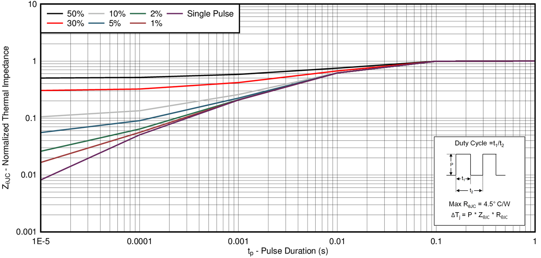
CSD17308Q3 D001_SLPS262.png
Figure 1. Transient Thermal Impedance
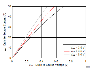
CSD17308Q3 D002_SLPS262.gif
Figure 2. Saturation Characteristics
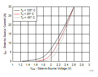
CSD17308Q3 D003_SLPS262.gif
VDS = 5 V
Figure 3. Transfer Characteristics
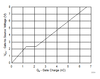
CSD17308Q3 D004_SLPS262.gif
ID = 10 A VDS = 15 V
Figure 4. Gate Charge
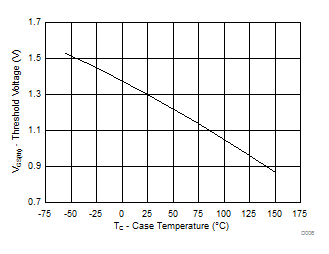
CSD17308Q3 D006_SLPS262.gif
ID = 250 µA
Figure 6. Threshold Voltage vs Temperature
CSD17308Q3 D008_SLPS262.gif
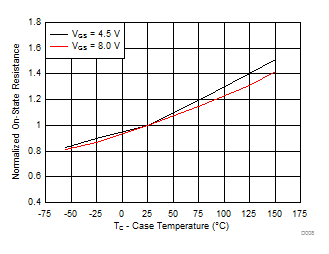
ID = 10 A VGS = 8 V
Figure 8. Normalized On-State Resistance vs Temperature
CSD17308Q3 D010_SLPS262.gif
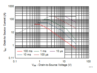
Single pulse, max RθJC = 4.5°C/W
Figure 10. Maximum Safe Operating Area
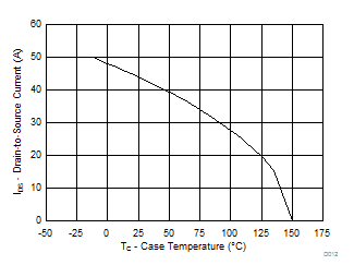
CSD17308Q3 D012_SLPS262.gif
Figure 12. Maximum Drain Current vs Temperature
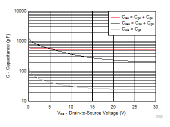
CSD17308Q3 D005_SLPS262.gif
Figure 5. Capacitance
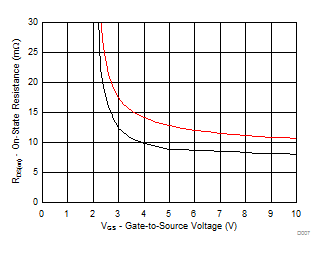
CSD17308Q3 D007_SLPS262.gif
ID = 10 A
Figure 7. On-State Resistance vs Gate-to-Source Voltage
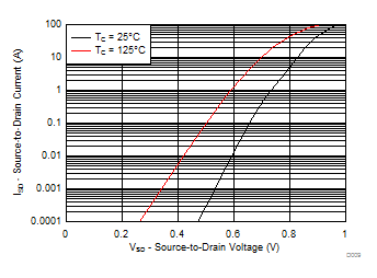
CSD17308Q3 D009_SLPS262.gif
Figure 9. Typical Diode Forward Voltage
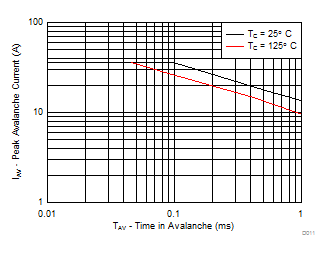
CSD17308Q3 D011_SLPS262.gif
Figure 11. Single Pulse Unclamped Inductive Switching