SLPS407C September   2013  – March 2017 CSD19531KCS

PRODUCTION DATA.  

  1. 1Features
  2. 2Applications
  3. 3Description
  4. 4Revision History
  5. 5Specifications
    1. 5.1 Electrical Characteristics
    2. 5.2 Thermal Information
    3. 5.3 Typical MOSFET Characteristics
  6. 6Device and Documentation Support
    1. 6.1 Receiving Notification of Documentation Updates
    2. 6.2 Community Resources
    3. 6.3 Trademarks
    4. 6.4 Electrostatic Discharge Caution
    5. 6.5 Glossary
  7. 7Mechanical, Packaging, and Orderable Information
    1. 7.1 KCS Package Dimensions

Package Options

Refer to the PDF data sheet for device specific package drawings

Mechanical Data (Package|Pins)
  • KCS|3
Thermal pad, mechanical data (Package|Pins)
Orderable Information

Specifications

Electrical Characteristics

TA = 25°C (unless otherwise stated)
PARAMETER TEST CONDITIONS MIN TYP MAX UNIT
STATIC CHARACTERISTICS
BVDSS Drain-to-source voltage VGS = 0 V, ID = 250 μA 100 V
IDSS Drain-to-source leakage current VGS = 0 V, VDS = 80 V 1 μA
IGSS Gate-to-source leakage current VDS = 0 V, VGS = 20 V 100 nA
VGS(th) Gate-to-source threshold voltage VDS = VGS, ID = 250 μA 2.2 2.7 3.3 V
RDS(on) Drain-to-source on resistance VGS = 6 V, ID = 60 A 7.3 8.8
VGS = 10 V, ID = 60 A 6.4 7.7
gfs Transconductance VDS = 10 V, ID = 60 A 137 S
DYNAMIC CHARACTERISTICS
Ciss Input capacitance VGS = 0 V, VDS = 50 V, ƒ = 1 MHz 2980 3870 pF
Coss Output capacitance 560 728 pF
Crss Reverse transfer capacitance 13 17 pF
RG Series gate resistance 1.3 2.6 Ω
Qg Gate charge total (10 V) VDS = 50 V, ID = 60 A 38 49 nC
Qgd Gate charge gate-to-drain 7.5 nC
Qgs Gate charge gate-to-source 11.9 nC
Qg(th) Gate charge at Vth 7.3 nC
Qoss Output charge VDS = 50 V, VGS = 0 V 98 nC
td(on) Turnon delay time VDS = 50 V, VGS = 10 V,
IDS = 60 A, RG = 0 Ω
8.4 ns
tr Rise Time 7.2 ns
td(off) Turnoff delay time 16 ns
tf Fall time 4.1 ns
DIODE CHARACTERISTICS
VSD Diode forward voltage ISD = 60 A, VGS = 0 V 0.9 1 V
Qrr Reverse recovery charge VDS= 50 V, IF = 60 A,
di/dt = 300 A/μs
270 nC
trr Reverse recovery time 83 ns

Thermal Information

TA = 25°C (unless otherwise stated)
THERMAL METRIC MIN TYP MAX UNIT
RθJC Junction-to-case thermal resistance 0.7 °C/W
RθJA Junction-to-ambient thermal resistance 62 °C/W

Typical MOSFET Characteristics

TA = 25°C (unless otherwise stated)
CSD19531KCS graph01F2_SLPS407.png
Figure 1. Transient Thermal Impedance
CSD19531KCS graph02_SLPS407.png
Figure 2. Saturation Characteristics
CSD19531KCS graph03_SLPS407.png
Figure 3. Transfer Characteristics
CSD19531KCS graph04F2_SLPS407.png
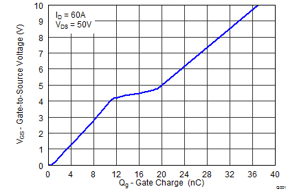
Figure 4. Gate Charge
CSD19531KCS graph06F2_SLPS407.png
Figure 6. Threshold Voltage vs Temperature
CSD19531KCS graph08F2_SLPS407.png
Figure 8. Normalized On-State Resistance vs Temperature
CSD19531KCS graph10F2_SLPS407.png
Figure 10. Maximum Safe Operating Area
CSD19531KCS graph12F2_SLPS407.png
Figure 12. Maximum Drain Current vs Temperature
CSD19531KCS graph05F_SLPS407.png
Figure 5. Capacitance
CSD19531KCS graph07_SLPS407.png
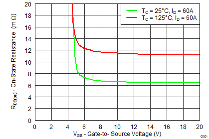
Figure 7. On-State Resistance vs Gate-to-Source Voltage
CSD19531KCS graph09_SLPS407.png
Figure 9. Typical Diode Forward Voltage
CSD19531KCS graph11_SLPS407.png
Figure 11. Single Pulse Unclamped Inductive Switching