SLPS666 March 2018 CSD86336Q3D
PRODUCTION DATA.
- 1Features
- 2Applications
- 3Description
- 4Revision History
-
5Specifications
- 5.1 Absolute Maximum Ratings
- 5.2 Recommended Operating Conditions
- 5.3 Thermal Information
- 5.4 Power Block Performance
- 5.5 Electrical Characteristics – Q1 Control FET
- 5.6 Electrical Characteristics – Q2 Sync FET
- 5.7 Typical Power Block Device Characteristics
- 5.8 Typical Power Block MOSFET Characteristics
- 6Application and Implementation
- 7Layout
- 8Device and Documentation Support
- 9Mechanical, Packaging, and Orderable Information
Package Options
Mechanical Data (Package|Pins)
- DPB|8
Thermal pad, mechanical data (Package|Pins)
Orderable Information
6.5.3 Calculating SOA Adjustments
- SOA adjustment for input voltage ≈ 1.0°C (Figure 5)
- SOA adjustment for output voltage ≈ 0.68°C (Figure 6)
- SOA adjustment for switching frequency ≈ 0.75°C (Figure 4)
- SOA adjustment for output inductor ≈ 0.02°C (Figure 7)
- Final calculated SOA adjustment = 1.0 + 0.68 + 0.75 + 0.02 ≈ 2.45°C
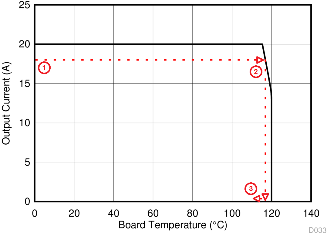
In the design example above, the estimated power loss of the CSD86336Q3D would increase to 3.85 W. In addition, the maximum allowable board and/or ambient temperature would have to decrease by 2.45°C. Figure 31 graphically shows how the SOA curve would be adjusted accordingly.
- Start by drawing a horizontal line from the application current to the SOA curve.
- Draw a vertical line from the SOA curve intercept down to the board/ambient temperature.
- Adjust the SOA board/ambient temperature by subtracting the temperature adjustment value.
In the design example, the SOA temperature adjustment yields a reduction in allowable board/ambient temperature of 2.45°C. In the event the adjustment value is a negative number, subtracting the negative number would yield an increase in allowable board/ambient temperature.
 Figure 31. Power Block SOA