SLPS666 March 2018 CSD86336Q3D
PRODUCTION DATA.
- 1Features
- 2Applications
- 3Description
- 4Revision History
-
5Specifications
- 5.1 Absolute Maximum Ratings
- 5.2 Recommended Operating Conditions
- 5.3 Thermal Information
- 5.4 Power Block Performance
- 5.5 Electrical Characteristics – Q1 Control FET
- 5.6 Electrical Characteristics – Q2 Sync FET
- 5.7 Typical Power Block Device Characteristics
- 5.8 Typical Power Block MOSFET Characteristics
- 6Application and Implementation
- 7Layout
- 8Device and Documentation Support
- 9Mechanical, Packaging, and Orderable Information
Package Options
Mechanical Data (Package|Pins)
- DPB|8
Thermal pad, mechanical data (Package|Pins)
Orderable Information
5.7 Typical Power Block Device Characteristics
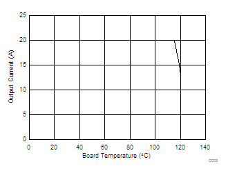
Test conditions: VIN = 12 V, VDD = 5 V, ƒSW = 500 kHz, VOUT = 1.3 V, LOUT = 0.95 µH, IOUT = 20 A, TJ = 125°C, unless stated otherwise.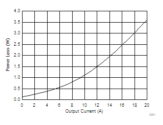
Figure 1. Power Loss vs Output Current
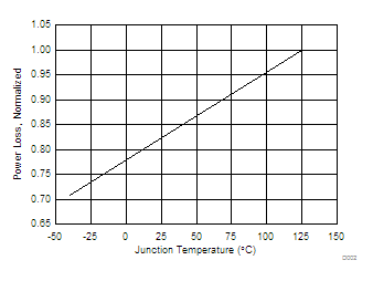
Figure 2. Power Loss vs Temperature
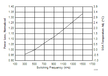
Figure 4. Normalized Power Loss vs Switching Frequency
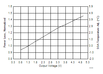
Figure 6. Normalized Power Loss vs Output Voltage
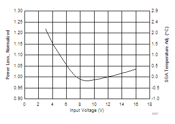
Figure 5. Normalized Power Loss vs Input Voltage
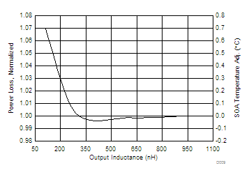
Figure 7. Normalized Power Loss vs Output Inductance
1. The Typical Power Block System Characteristic curves are based on measurements made on a PCB design with dimensions of 4 in (W) × 3.5 in (L) × 0.062 in (H) and 6 copper layers of 1-oz copper thickness. See Application and Implementation section for detailed explanation.
