SLPS642 April 2017 CSD87313DMS
PRODUCTION DATA.
- 1Features
- 2Applications
- 3Description
- 4Revision History
- 5 Specifications
- 6Device and Documentation Support
- 7Mechanical, Packaging, and Orderable Information
Package Options
Refer to the PDF data sheet for device specific package drawings
Mechanical Data (Package|Pins)
- DMS|8
Thermal pad, mechanical data (Package|Pins)
Orderable Information
7 Mechanical, Packaging, and Orderable Information
The following pages include mechanical, packaging, and orderable information. This information is the most current data available for the designated devices. This data is subject to change without notice and revision of this document. For browser-based versions of this data sheet, refer to the left-hand navigation.
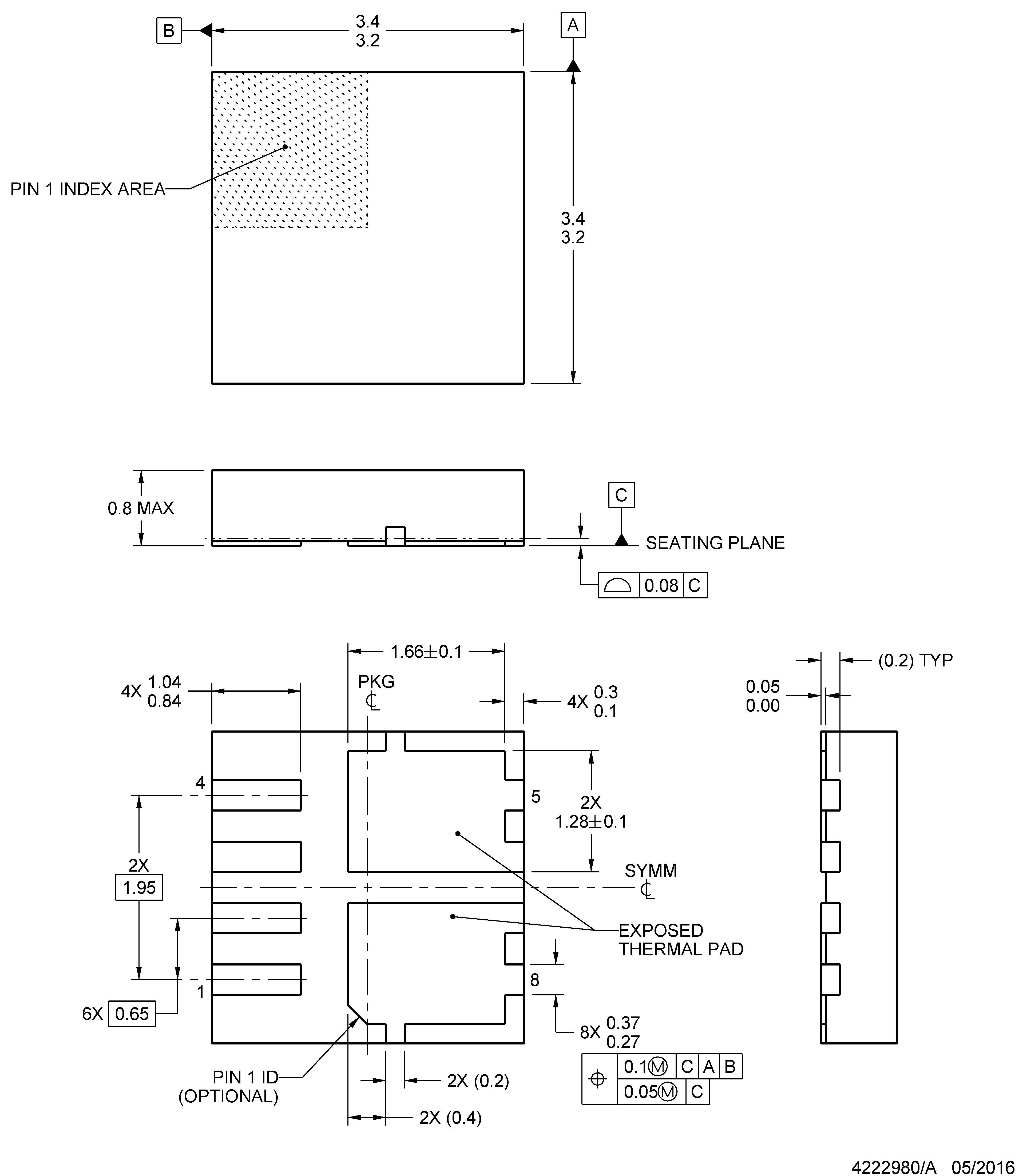
7.1 DMS Package Dimensions

1. All linear dimensions are in millimeters. Any dimensions in parenthesis are for reference only. Dimensioning and tolerancing per ASME Y14.5M.
2. This drawing is subject to change without notice.
3. The package thermal pad must be soldered to the printed circuit board for thermal and mechanical performance.
Table 1. Pin Configuration Table
| POSITION | DESIGNATION | POSITION | DESIGNATION |
|---|---|---|---|
| 1 | Gate 1 | 5 | Source 2 |
| 2 | Drain | 6 | Source 2 |
| 3 | Drain | 7 | Source 1 |
| 4 | Gate 2 | 8 | Source 1 |
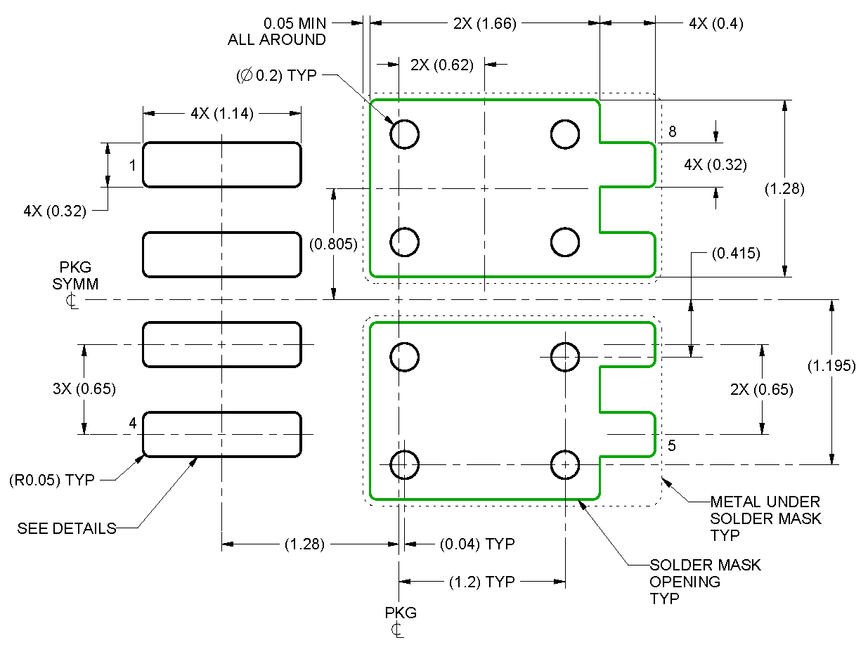
7.2 Recommended PCB Pattern


1. This package is designed to be soldered to a thermal pad on the board. For more information, see QFN/SON PCB Attachment (SLUA271).
2. Vias are optional depending on application, refer to device data sheet. If any vias are implemented, refer to their locations shown on this view. It is recommended that vias under paste be filled, plugged or tented.
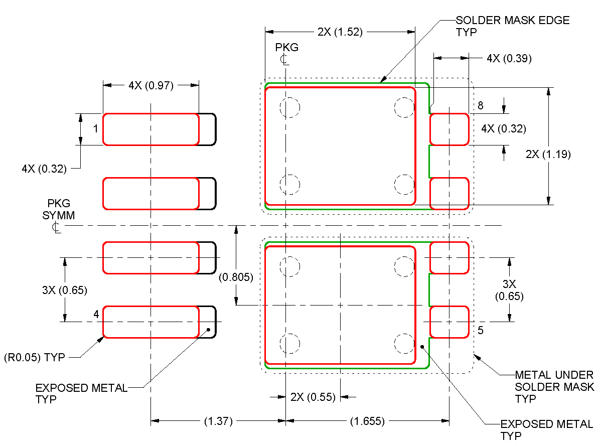
7.3 Recommended Stencil Opening

1. Laser cutting apertures with trapezoidal walls and rounded corners may offer better paste release. IPC-7525 may have alternate design recommendations.