SLPS455A January 2014 – August 2014 CSD88537ND
PRODUCTION DATA.
- 1Features
- 2Applications
- 3Description
- 4Revision History
- 5Specifications
- 6Device and Documentation Support
- 7Mechanical, Packaging, and Orderable Information
Package Options
Refer to the PDF data sheet for device specific package drawings
Mechanical Data (Package|Pins)
- D|8
Thermal pad, mechanical data (Package|Pins)
Orderable Information
7 Mechanical, Packaging, and Orderable Information
The following pages include mechanical, packaging, and orderable information. This information is the most current data available for the designated devices. This data is subject to change without notice and revision of this document. For browser-based versions of this data sheet, refer to the left-hand navigation.
7.1 SO-8 Package Dimensions
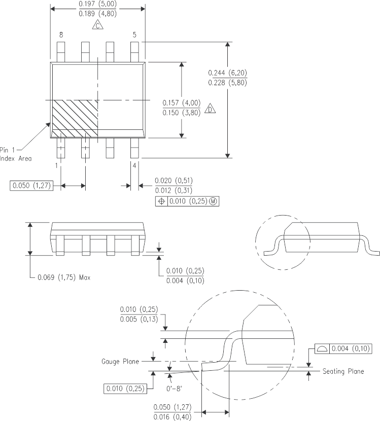
- All linear dimensions are in inches (millimeters).
- This drawing is subject to change without notice.
- Body length does not include mold flash, protrusions, or gate burrs. Mold flash, protrusions, or gate burrs shall not exceed 0.006 (0.15) each side.
- Body width does not include interlead flash. Interlead flash shall not exceed 0.017 (0.43) each side.
- Reference JEDEC MS-012 variation AA.
7.2 Recommended PCB Pattern and Stencil Opening
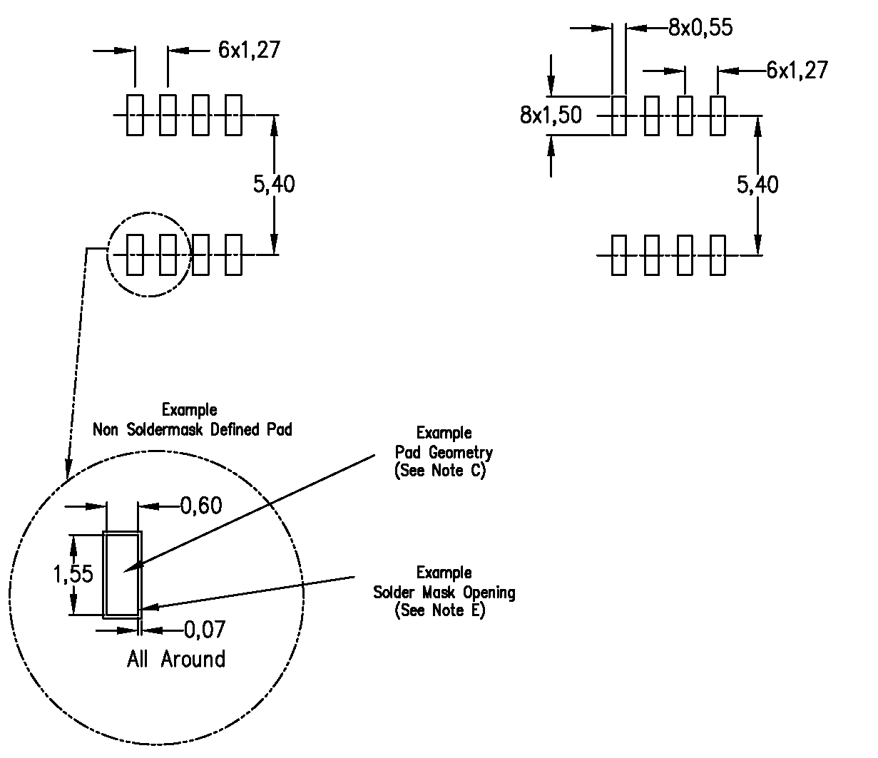
- All linear dimensions are in millimeters.
- This drawing is subject to change without notice.
- Publication IPC-7351 is recommended for alternate designs.
- Laser cutting apertures with trapezoidal walls and also rounding corners will offer better paste release. Customers should contact their board assembly site for stencil design recommendations. Refer to IPC-7525 for other stencil recommendations.
- Customers should contact their board fabrication site for solder mask tolerances between and around signal pads.