SLAS452E October 2020 – January 2021 DAC5652
PRODUCTION DATA
- 1 Features
- 2 Applications
- 3 Description
- 4 Revision History
- 5 Pin Configuration and Functions
-
6 Specifications
- 6.1 Absolute Maximum Rationgs
- 6.2 ESD Ratings
- 6.3 Recommended Operating Conditions
- 6.4 Thermal Resistance Characteristics
- 6.5 Electrical Characteristics
- 6.6 Electrical Characteristics
- 6.7 Electrical Characteristics, AC
- 6.8 Electrical Characteristics, DC
- 6.9 Switching Characteristics
- 6.10 Typical Characteristics
- 7 Parameter Measurement Information
- 8 Detailed Description
- 9 Application Information Disclaimer
- 10Power Supply Recommendations
- 11Layout
- 12Device and Documentation Support
- 13Mechanical, Packaging, and Orderable Information
Package Options
Mechanical Data (Package|Pins)
- PFB|48
Thermal pad, mechanical data (Package|Pins)
- PFB|48
Orderable Information
3 Description
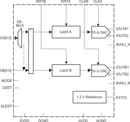
The DAC5652 is a monolithic, dual-channel, 10-bit, high-speed DAC with on-chip voltage reference.
Operating with update rates of up to 275 MSPS, the DAC5652 offers exceptional dynamic performance, tight-gain, and offset matching characteristics that make it suitable in either I/Q baseband or direct IF communication applications.
Each DAC has a high-impedance, differential-current output, suitable for single-ended or differential analog-output configurations. External resistors allow scaling of the full-scale output current for each DAC separately or together, typically between 2 mA and 20 mA. An accurate on-chip voltage reference is temperature-compensated and delivers a stable 1.2-V reference voltage. Optionally, an external reference may be used.
The DAC5652 has two, 10-bit, parallel input ports with separate clocks and data latches. For flexibility, the DAC5652 also supports multiplexed data for each DAC on one port when operating in the interleaved mode.
The DAC5652 has been specifically designed for a differential transformer-coupled output with a 50-Ω doubly-terminated load. For a 20-mA full-scale output current, both a 4:1 impedance ratio (resulting in an output power of 4 dBm) and 1:1 impedance ratio transformer (–2 dBm output power) are supported.
The DAC5652 is available in a 48-pin TQFP package. Pin compatibility between family members provides 10-bit (DAC5652), 12-bit (DAC5662), and 14-bit (DAC5672) resolution. Furthermore, the DAC5652 is pin compatible to the DAC2900 and AD9763 dual DACs. The device is characterized for operation over the industrial temperature range of –40°C to 85°C.
| PART NUMBER | PACKAGE(1) | BODY SIZE (NOM) |
|---|---|---|
| DAC5652 | TQFP | 7.00 mm x 7.00 mm |
 Functional Block Diagram