SLAS528B August 2017 – January 2018 DAC5672A
PRODUCTION DATA.
- 1 Features
- 2 Applications
- 3 Description
- 4 Revision History
- 5 Pin Configuration and Functions
-
6 Specifications
- 6.1 Absolute Maximum Ratings
- 6.2 ESD Ratings
- 6.3 Recommended Operating Conditions
- 6.4 Thermal Information
- 6.5 Electrical Characteristics
- 6.6 Electrical Characteristics
- 6.7 Electrical Characteristics: AC Characteristics
- 6.8 Electrical Characteristics: Digital Characteristics
- 6.9 Switching Characteristics
- 6.10 Typical Characteristics
- 7 Detailed Description
- 8 Application and Implementation
- 9 Power Supply Recommendations
- 10Layout
- 11Device and Documentation Support
- 12Mechanical, Packaging, and Orderable Information
Package Options
Mechanical Data (Package|Pins)
- PFB|48
Thermal pad, mechanical data (Package|Pins)
Orderable Information
10 Layout
10.1 Layout Guidelines
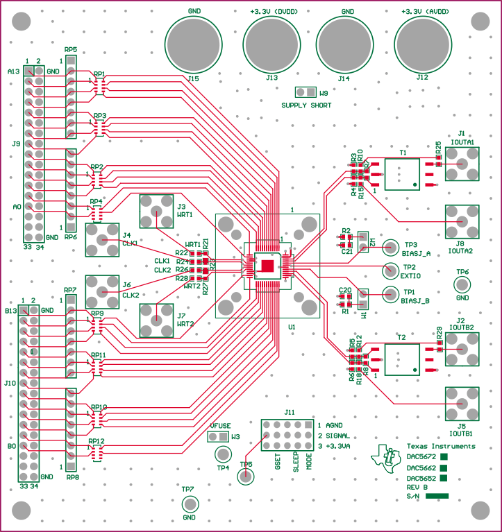
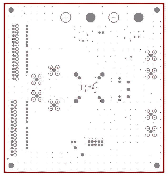
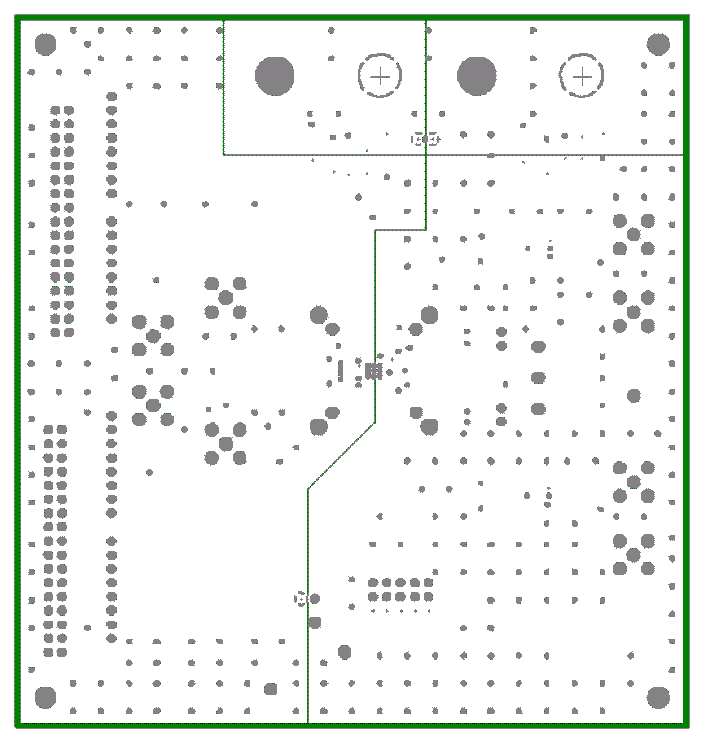
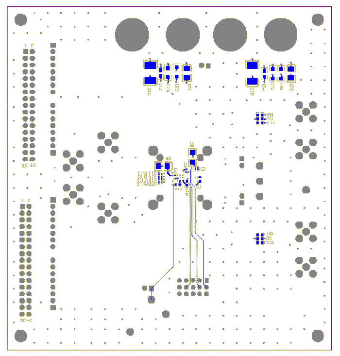
The DAC5672A EVM layout should be used as a reference for the layout to obtain the best performance. A sample layout is shown in Figure 27 through Figure 30. Some important layout recommendations are:
- Use a single ground plane. Keep the digital and analog signals on distinct separate sections of the board. This may be virtually divided down the middle of the device package when doing placement and layout.
- Keep the analog outputs as far away from the switching clocks and digital signals as possible. This will keep coupling from the digital circuits to the analog outputs to a minimum.
- Decoupling caps should be kept close to the power pins of the device.
10.2 Layout Example
The EVM is constructed on a 4-layer, 5.1-inch x 4.8-inch, 0.062-inch thick PCB using FR−4 material. Figure 27 through Figure 30 show the PCB layout for the EVM.
 Figure 27. Top Layer 1
 Figure 28. Ground Plane Layer 2
 Figure 29. Power Plane Layer 3
 Figure 30. Bottom Layer 4