SGLS387H July 2007 – August 2016 DAC5675A-SP
PRODUCTION DATA.
- 1 Features
- 2 Applications
- 3 Description
- 4 Revision History
- 5 Description (continued)
- 6 Pin Configuration and Functions
-
7 Specifications
- 7.1 Absolute Maximum Ratings
- 7.2 ESD Ratings
- 7.3 Recommended Operating Conditions
- 7.4 Thermal Information
- 7.5 DC Electrical Characteristics (Unchanged After 100 kRad)
- 7.6 AC Electrical Characteristics (Unchanged After 100 kRad)
- 7.7 Digital Specifications (Unchanged After 100 kRad)
- 7.8 Electrical Characteristics
- 7.9 Typical Characteristics
- 8 Detailed Description
- 9 Application and Implementation
- 10Power Supply Recommendations
- 11Layout
- 12Device and Documentation Support
- 13Mechanical, Packaging, and Orderable Information
Package Options
Refer to the PDF data sheet for device specific package drawings
Mechanical Data (Package|Pins)
- HFG|52
Thermal pad, mechanical data (Package|Pins)
Orderable Information
9 Application and Implementation
NOTE
Information in the following applications sections is not part of the TI component specification, and TI does not warrant its accuracy or completeness. TI’s customers are responsible for determining suitability of components for their purposes. Customers should validate and test their design implementation to confirm system functionality.
9.1 Application Information
The DAC5675A-SP is a 14-bit resolution high-speed DAC. The DAC5675A-SP is designed for high-speed digital data transmission in wired and wireless communication systems, high-frequency DDS, and waveform reconstruction in test and measurement applications. The DAC5675A-SP has excellent SFDR at high intermediate frequencies, which makes it well suited for multicarrier transmission in TDMA and CDMA based cellular BTSs.
9.2 Typical Application
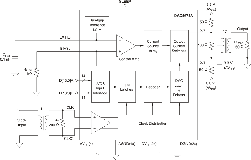
The DAC5675A-SP consists of a segmented array of NPN-transistor current sources, capable of delivering a full-scale output current up to 20 mA. Differential current switches direct the current of each current source to either one of the complementary output nodes IOUT1 or IOUT2. The complementary current output enables differential operation, canceling out common-mode noise sources (digital feed through, on-chip, and PCB noise), dc offsets, and even order distortion components, and doubling signal output power.
 Figure 22. Typical Application Schematic
9.2.1 Design Requirements
For this design example, use the parameters listed in Table 1 as the input parameters.
Table 1. Design Parameters
| Design Parameter | Example Value |
|---|---|
| Cest | 0.1 µF |
| Rbias | 1 kΩ |
| RT | 200 Ω |
| Rload | 50 Ω |
9.2.2 Detailed Design Procedure
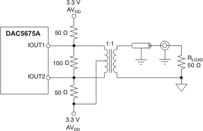
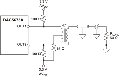
The DAC5675A-SP can be easily configured to drive a doubly-terminated 50-Ω cable using a properly selected transformer. Figure 23 and Figure 24 show the 1:1 and 4:1 impedance ratio configuration, respectively. These configurations provide maximum rejection of common-mode noise sources and even-order distortion components, thereby doubling the power of the DAC to the output. The center tap on the primary side of the transformer is terminated to AVDD, enabling a dc-current flow for both IOUT1 and IOUT2. Note that the ac performance of the DAC5675A-SP is optimum and specified using a 1:1 differential transformer-coupled output.
 Figure 23. Driving a Doubly Terminated 50-Ω Cable Using a 1:1 Impedance Ratio Transformer
 Figure 24. Driving a Doubly Terminated 50 Ω Cable Using a 4:1 Impedance Ratio Transformer
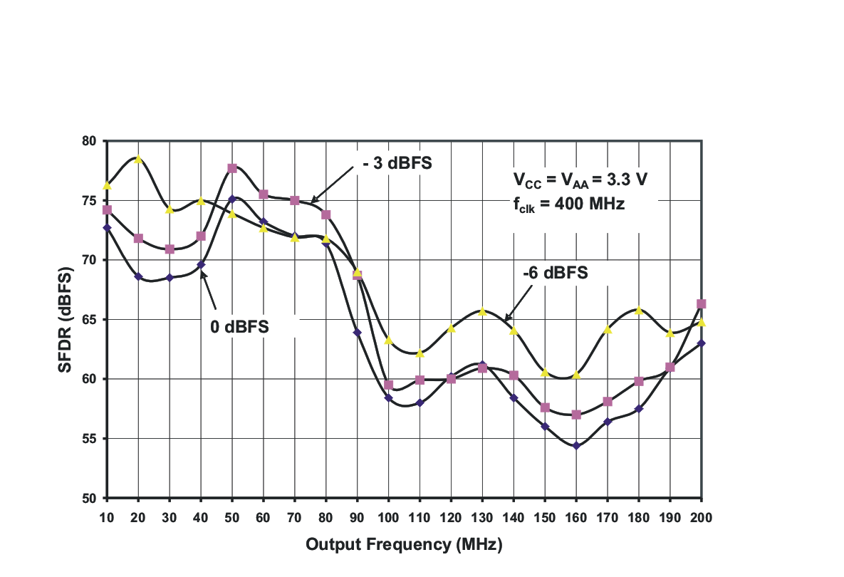
9.2.3 Application Curve
