DLPS030E December 2013 – March 2019 DLPC2607
PRODUCTION DATA.
- 1 Features
- 2 Applications
- 3 Description
- 4 Revision History
- 5 Pin Configuration and Functions
-
6 Specifications
- 6.1 Absolute Maximum Ratings
- 6.2 ESD Ratings
- 6.3 Recommended Operating Conditions
- 6.4 Thermal Information
- 6.5 Typical Current and Power Dissipation
- 6.6 I/O Characteristics
- 6.7 Internal Pullup and Pulldown Characteristics
- 6.8 Parallel I/F Frame Timing Requirements
- 6.9 Parallel I/F General Timing Requirements
- 6.10 Parallel I/F Maximum Parallel Interface Horizontal Line Rate
- 6.11 BT.656 I/F General Timing Requirements
- 6.12 100- to 120-Hz Operational Limitations
- 6.13 Flash Interface Timing Requirements
- 6.14 DMD Interface Timing Requirements
- 6.15 mDDR Memory Interface Timing Requirements
- 7 Detailed Description
- 8 Application and Implementation
- 9 Power Supply Recommendations
-
10Layout
- 10.1
Layout Guidelines
- 10.1.1 Internal ASIC PLL Power
- 10.1.2 General Handling Guidelines for Unused CMOS-Type Pins
- 10.1.3 SPI Signal Routing
- 10.1.4 mDDR Memory and DMD Interface Considerations
- 10.1.5 PCB Design
- 10.1.6 General PCB Routing (Applies to All Corresponding PCB Signals)
- 10.1.7 Maximum, Pin-to-Pin, PCB Interconnects Etch Lengths
- 10.1.8 I/F Specific PCB Routing
- 10.1.9 Number of Layer Changes
- 10.1.10 Stubs
- 10.1.11 Termination Requirements:
- 10.2 Layout Example
- 10.1
Layout Guidelines
- 11Device and Documentation Support
- 12Mechanical, Packaging, and Orderable Information
Refer to the PDF data sheet for device specific package drawings
Mechanical Data (Package|Pins)
- ZVB|176
Thermal pad, mechanical data (Package|Pins)
8.2 Typical Application
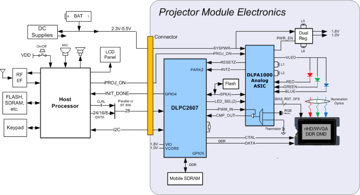
Figure 10 shows a typical accessory projector application. For this application, the DLPC2607 device is controlled by a separate control processor (typically a MSP430) and the image data is received from a TVP5151 video decoder device. For this application, the ASIC supports periodic sources only. A common application when using DLPC2607 controller is for creating an accessory Pico projector for a smartphone, tablets or any other display source. The DLPC2607 in the accessory Pico projector typically receives images from a host processor or a multimedia processor.
 Figure 10. Typical Standalone Projector System Block Diagram