DLPS029F April   2013  – May 2019 DLPC350

PRODUCTION DATA.  

  1. Features
  2. Applications
  3. Description
    1.     Simplified Application
  4. Revision History
  5. Pin Configuration and Functions
    1.     Pin Functions
    2. Table 1. Power and Ground Pin Descriptions
  6. Specifications
    1. 6.1  Absolute Maximum Ratings
    2. 6.2  ESD Ratings
    3. 6.3  Recommended Operating Conditions
    4. 6.4  Thermal Information
    5. 6.5  I/O Electrical Characteristics
    6. 6.6  I2C0 and I2C1 Interface Timing Requirements
    7. 6.7  Port 1 Input Pixel Interface Timing Requirements
    8. 6.8  Port 2 Input Pixel Interface (FPD-Link Compatible LVDS Input) Timing Requirements
    9. 6.9  System Oscillator Timing Requirements
    10. 6.10 Reset Timing Requirements
    11. 6.11 Video Timing Input Blanking Specification
      1. 6.11.1 Source Input Blanking
    12. 6.12 Programmable Output Clocks Switching Characteristics
    13. 6.13 DMD Interface Switching Characteristics
    14. 6.14 JTAG Interface: I/O Boundary Scan Application Switching Characteristics
  7. Parameter Measurement Information
    1. 7.1 Power Consumption
  8. Detailed Description
    1. 8.1 Overview
    2. 8.2 Functional Block Diagram
    3. 8.3 Feature Description
      1. 8.3.1 Board Level Test Support
    4. 8.4 Device Functional Modes
      1. 8.4.1 Structured Light Applications
      2. 8.4.2 (LVDS) Receiver Supported Pixel Mapping Modes
  9. Application and Implementation
    1. 9.1 Application Information
    2. 9.2 Typical Applications
      1. 9.2.1 Typical Chipset Application
        1. 9.2.1.1 Design Requirements
        2. 9.2.1.2 Detailed Design Procedure
          1. 9.2.1.2.1 DLPC350 System Interfaces
            1. 9.2.1.2.1.1 Control Interface
            2. 9.2.1.2.1.2 Input Data Interface
          2. 9.2.1.2.2 DLPC350 System Output Interfaces
            1. 9.2.1.2.2.1 Illumination Interface
            2. 9.2.1.2.2.2 Trigger Interface (Sync Outputs)
          3. 9.2.1.2.3 DLPC350 System Support Interfaces
            1. 9.2.1.2.3.1 Reference Clock
            2. 9.2.1.2.3.2 PLL
            3. 9.2.1.2.3.3 Program Memory Flash Interface
          4. 9.2.1.2.4 DMD Interfaces
            1. 9.2.1.2.4.1 DLPC350 to DMD Digital Data
            2. 9.2.1.2.4.2 DLPC350 to DMD Control Interface
            3. 9.2.1.2.4.3 DLPC350 to DMD Micromirror Reset Control Interface
  10. 10Power Supply Recommendations
    1. 10.1 System Power and Reset
      1. 10.1.1 Default Conditions
        1. 10.1.1.1 1.2-V System Power
        2. 10.1.1.2 1.8-V System Power
        3. 10.1.1.3 1.9-V System Power
        4. 10.1.1.4 3.3-V System Power
        5. 10.1.1.5 FPD-Link Input LVDS System Power
      2. 10.1.2 System Power-up and Power-down Sequence
      3. 10.1.3 Power-On Sense (POSENSE) Support
      4. 10.1.4 Power-Good (PWRGOOD) Support
      5. 10.1.5 5-V Tolerant Support
      6. 10.1.6 Power Reset Operation
      7. 10.1.7 System Reset Operation
  11. 11Layout
    1. 11.1 Layout Guidelines
      1. 11.1.1 DMD Interface Design Considerations
      2. 11.1.2 DMD Termination Requirements
      3. 11.1.3 Decoupling Capacitors
      4. 11.1.4 Power Plane Recommendations
      5. 11.1.5 Signal Layer Recommendations
      6. 11.1.6 General Handling Guidelines for CMOS-Type Pins
      7. 11.1.7 PCB Manufacturing
        1. 11.1.7.1 General Guidelines
        2. 11.1.7.2 Trace Widths and Minimum Spacings
        3. 11.1.7.3 Routing Constraints
        4. 11.1.7.4 Fiducials
        5. 11.1.7.5 Flex Considerations
        6. 11.1.7.6 DLPC350 Thermal Considerations
    2. 11.2 Layout Example
      1. 11.2.1 Printed Circuit Board Layer Stackup Geometry
      2. 11.2.2 Recommended DLPC350 MOSC Crystal Oscillator Configuration
      3. 11.2.3 Recommended DLPC350 PLL Layout Configuration
  12. 12Device and Documentation Support
    1. 12.1 Device Support
      1. 12.1.1 Video Timing Parameter Definitions
      2. 12.1.2 Device Nomenclature
      3. 12.1.3 Device Marking
    2. 12.2 Documentation Support
      1. 12.2.1 Related Documentation
    3. 12.3 Trademarks
    4. 12.4 Glossary
  13. 13Mechanical, Packaging, and Orderable Information
    1. 13.1 Package Option Addendum
      1. 13.1.1 Packaging Information

Package Options

Mechanical Data (Package|Pins)
Thermal pad, mechanical data (Package|Pins)

Description

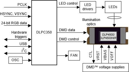
The DLPC350 digital controller is required for reliable operation of the DLP4500 or DLP4500NIR digital micromirror device (DMD). The DLPC350 controller provides a convenient, multi-functional interface between user electronics and the DMD, enabling high-speed pattern rates, along with LED control and data formatting for multiple input formats.

The DLPC350 controller provides input and output trigger signals for synchronizing displayed patterns with a camera, sensor, or other peripherals. The controller enables integration into small-form-factor and low-cost light steering applications. Applications include 3D scanning or metrology systems, spectrometers, interactive displays, chemical analyzers, medical instruments, and other end equipment that requires spatial light modulation (light steering and patterning).

The DLPC350 controller is the data formatting and DMD controlling ASIC for either the visible or near-infrared (NIR) version of the DLP4500. For further details, please see the DLPR350 firmware homepage, the DLP4500 data sheet, and the DLP4500NIR data sheet.

Device Information(1)

ORDER NUMBER PACKAGE BODY SIZE
DLPC350 BGA (419) 23.4 mm × 23.4 mm
  1. For all available packages, see the orderable addendum at the end of the data sheet.

Simplified Application
DLPC350 simp_app_dlps029.gif