SLVSBN6A June 2013 – August 2015 DRV201A
PRODUCTION DATA.
- 1 Features
- 2 Applications
- 3 Description
- 4 Revision History
- 5 Pin Configuration and Functions
- 6 Specifications
-
7 Detailed Description
- 7.1 Overview
- 7.2 Functional Block Diagram
- 7.3 Feature Description
- 7.4 Device Functional Modes
- 7.5 Programming
- 7.6
Register Maps
- 7.6.1 Control Register (Address - 0x02h)
- 7.6.2 VCM MSB Current Control Register (VCM_Current_MSB) Address - 0x03h
- 7.6.3 VCM LSB Current Control Register (VCM_Current_lSB) Address - 0x04h
- 7.6.4 Status Register (Status) Address - 0x05h
- 7.6.5 Mode Register (Mode) Address - 0x06h
- 7.6.6 VCM Resonance Frequency Register (VCM_FREQ) Address - 0x07h
- 8 Application and Implementation
- 9 Power Supply Recommendations
- 10Layout
- 11Device and Documentation Support
- 12Mechanical, Packaging, and Orderable Information
Package Options
Mechanical Data (Package|Pins)
- YMB|6
Thermal pad, mechanical data (Package|Pins)
Orderable Information
5 Pin Configuration and Functions
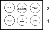
YMB Package
6-Pin PicoStar
Bottom View

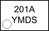
YMB Package
6-Pin PicoStar
Top View

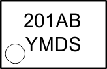
YMB Package
6-Pin PicoStar
Top View

The coated package option has a backside polymer coating that is 40µm thick. The final package heights of both the packages are the same for both options. This coating helps minimize edge chipping or die cracking during assembly and manufacturing.
Pin Functions
| PIN | I/O | DESCRIPTION | |
|---|---|---|---|
| NAME | NO. | ||
| VBAT | 2A | — | Power |
| GND | 1A | — | Ground |
| I_SOURCE | 2B | — | Voice coil positive terminal |
| I_SINK | 1B | — | Voice coil negative terminal |
| SCL | 2C | I | I2C serial interface clock input |
| SDA | 1C | I/O | I2C serial interface data input/output (open drain) |