SLVSDX8B March   2017  – December 2018 DRV8702D-Q1 , DRV8703D-Q1

PRODUCTION DATA.  

  1. Features
  2. Applications
  3. Description
    1.     Device Images
      1.      Simplified Schematic
  4. Revision History
  5. Pin Configuration and Functions
    1.     Pin Functions
  6. Specifications
    1. 6.1 Absolute Maximum Ratings
    2. 6.2 ESD Ratings
    3. 6.3 Recommended Operating Conditions
    4. 6.4 Thermal Information
    5. 6.5 Electrical Characteristics
    6. 6.6 SPI Timing Requirements
    7. 6.7 Switching Characteristics
    8. 6.8 Typical Characteristics
  7. Detailed Description
    1. 7.1 Overview
    2. 7.2 Functional Block Diagram
    3. 7.3 Feature Description
      1. 7.3.1  Bridge Control
        1. 7.3.1.1 Logic Tables
      2. 7.3.2  MODE Pin
      3. 7.3.3  nFAULT Pin
      4. 7.3.4  Current Regulation
      5. 7.3.5  Amplifier Output (SO)
        1. 7.3.5.1 SO Sample and Hold Operation
      6. 7.3.6  PWM Motor Gate Drivers
        1. 7.3.6.1 Miller Charge (QGD)
      7. 7.3.7  IDRIVE Pin (DRV8702D-Q1 Only)
      8. 7.3.8  Dead Time
      9. 7.3.9  Propagation Delay
      10. 7.3.10 Overcurrent VDS Monitor
      11. 7.3.11 VDS Pin (DRV8702D-Q1 Only)
      12. 7.3.12 Charge Pump
      13. 7.3.13 Gate Drive Clamp
      14. 7.3.14 Protection Circuits
        1. 7.3.14.1 VM Undervoltage Lockout (UVLO2)
        2. 7.3.14.2 Logic Undervoltage (UVLO1)
        3. 7.3.14.3 VCP Undervoltage Lockout (CPUV)
        4. 7.3.14.4 Overcurrent Protection (OCP)
        5. 7.3.14.5 Gate Driver Fault (GDF)
        6. 7.3.14.6 Thermal Shutdown (TSD)
        7. 7.3.14.7 Watchdog Fault (WDFLT, DRV8703D-Q1 Only)
        8. 7.3.14.8 Reverse Supply Protection
      15. 7.3.15 Hardware Interface
        1. 7.3.15.1 IDRIVE (6-level input)
        2. 7.3.15.2 VDS (6-Level Input)
    4. 7.4 Device Functional Modes
    5. 7.5 Programming
      1. 7.5.1 SPI Communication
        1. 7.5.1.1 Serial Peripheral Interface (SPI)
        2. 7.5.1.2 SPI Format
    6. 7.6 Register Maps
      1. 7.6.1 DRV8703D-Q1 Memory Map
      2. 7.6.2 Status Registers
        1. 7.6.2.1 FAULT Status Register (address = 0x00h)
          1. Table 15. FAULT Status Field Descriptions
        2. 7.6.2.2 VDS and GDF Status Register Name (address = 0x01h)
          1. Table 16. VDS and GDF Status Field Descriptions
      3. 7.6.3 Control Registers
        1. 7.6.3.1 Main Control Register Name (address = 0x02h)
          1. Table 18. Main Control Field Descriptions
        2. 7.6.3.2 IDRIVE and WD Control Register Name (address = 0x03h)
          1. Table 19. IDRIVE and WD Field Descriptions
        3. 7.6.3.3 VDS Control Register Name (address = 0x04h)
          1. Table 21. VDS Control Field Descriptions
        4. 7.6.3.4 Config Control Register Name (address = 0x05h)
          1. Table 22. Config Control Field Descriptions
  8. Application and Implementation
    1. 8.1 Application Information
    2. 8.2 Typical Application
      1. 8.2.1 Design Requirements
      2. 8.2.2 Detailed Design Procedure
        1. 8.2.2.1 External FET Selection
        2. 8.2.2.2 IDRIVE Configuration
        3. 8.2.2.3 VDS Configuration
        4. 8.2.2.4 Current Chopping Configuration
      3. 8.2.3 Application Curves
  9. Power Supply Recommendations
    1. 9.1 Bulk Capacitance Sizing
  10. 10Layout
    1. 10.1 Layout Guidelines
    2. 10.2 Layout Example
  11. 11Device and Documentation Support
    1. 11.1 Documentation Support
      1. 11.1.1 Related Documentation
    2. 11.2 Related Links
    3. 11.3 Receiving Notification of Documentation Updates
    4. 11.4 Community Resources
    5. 11.5 Trademarks
    6. 11.6 Electrostatic Discharge Caution
    7. 11.7 Glossary
  12. 12Mechanical, Packaging, and Orderable Information

Package Options

Refer to the PDF data sheet for device specific package drawings

Mechanical Data (Package|Pins)
  • RHB|32
Thermal pad, mechanical data (Package|Pins)
Orderable Information

Mechanical, Packaging, and Orderable Information

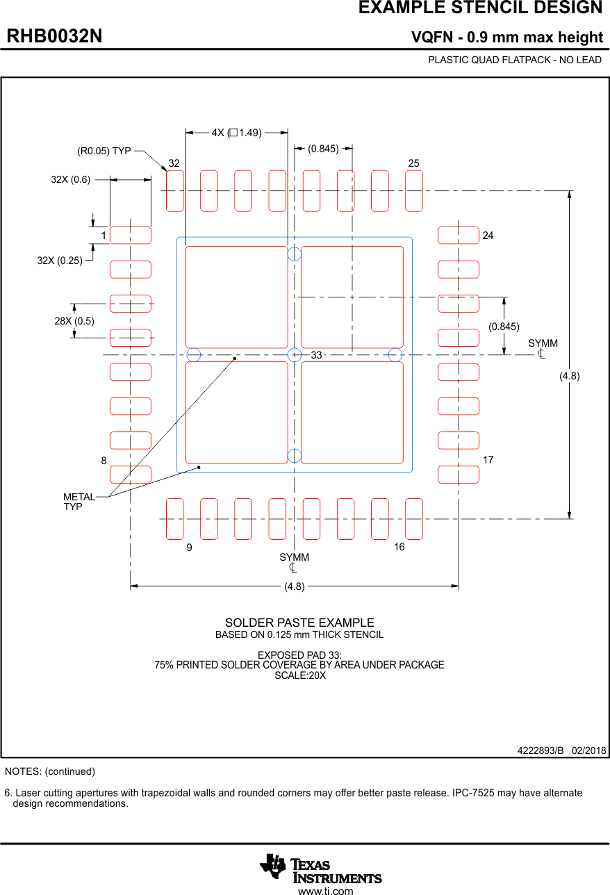
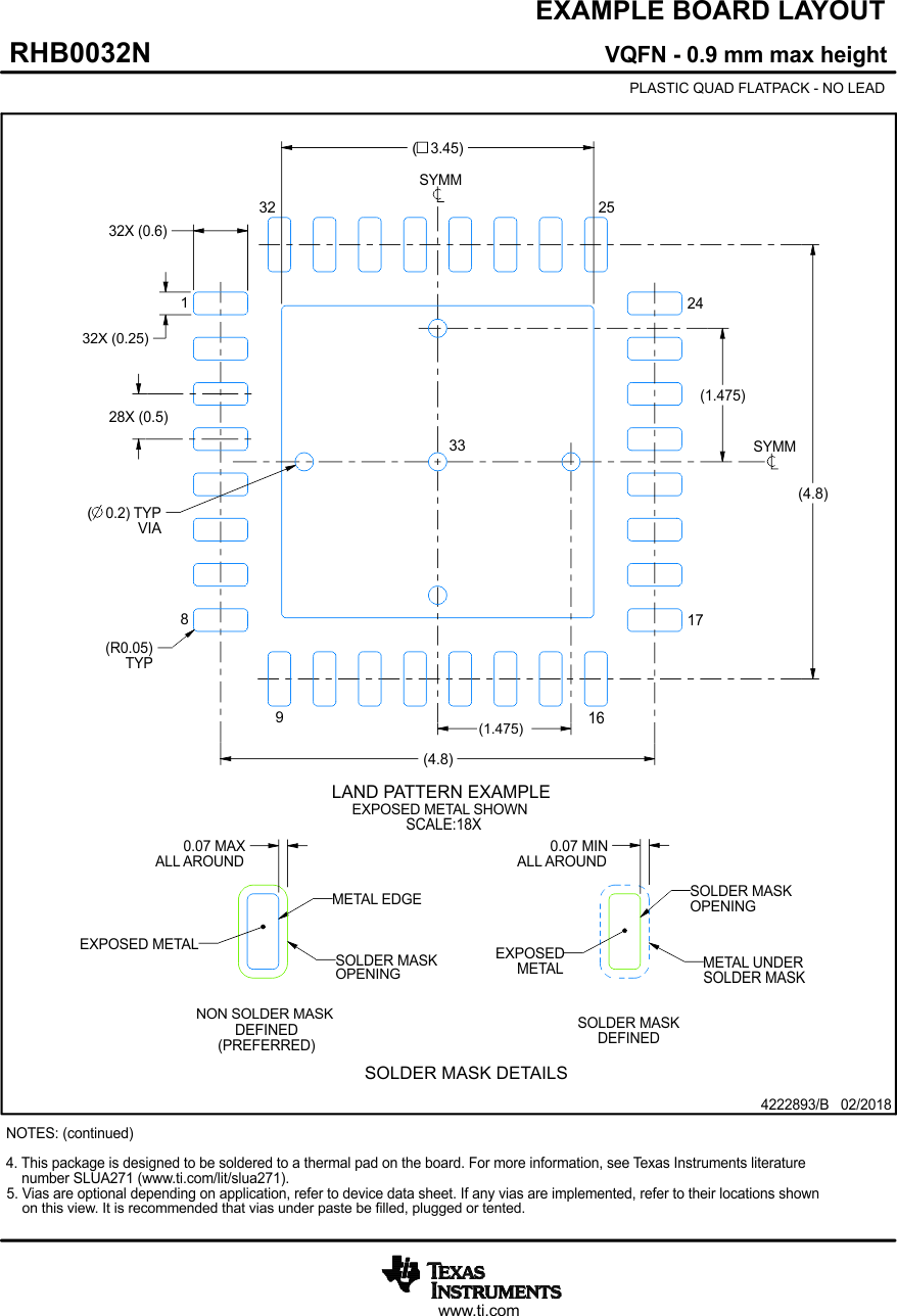
The following pages include mechanical, packaging, and orderable information. This information is the most current data available for the designated devices. This data is subject to change without notice and revision of this document. For browser-based versions of this data sheet, refer to the left-hand navigation.
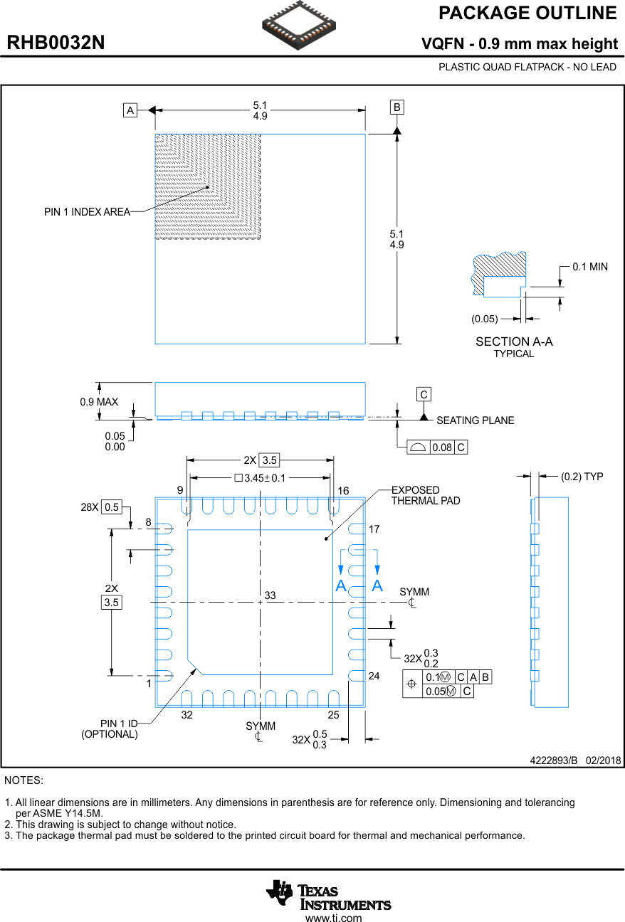
DRV8702D-Q1 DRV8703D-Q1 RHB0032N_4222893_Page_01.gif
DRV8702D-Q1 DRV8703D-Q1 RHB0032N_4222893_Page_02.gif
DRV8702D-Q1 DRV8703D-Q1 RHB0032N_4222893_Page_03.gif