SLVSCI2A June 2014 – June 2014 DRV8802-Q1
PRODUCTION DATA.
- 1 Features
- 2 Applications
- 3 Description
- 4 Revision History
- 5 Pin Configuration and Functions
- 6 Specifications
- 7 Detailed Description
- 8 Application and Implementation
- 9 Power Supply Recommendations
- 10Layout
- 11Device and Documentation Support
- 12Mechanical, Packaging, and Orderable Information
Package Options
Mechanical Data (Package|Pins)
- PWP|28
Thermal pad, mechanical data (Package|Pins)
- PWP|28
Orderable Information
8 Application and Implementation
8.1 Application Information
The DRV8802-Q1 device is used in medium voltage brushed-DC motor control applications.
8.2 Typical Application
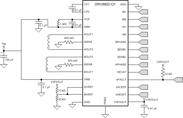 Figure 7. Typical Application Diagram
8.2.1 Design Requirements
The example supply for this design is V(VMx) = 18 V.
8.2.2 Detailed Design Procedure
8.2.2.1 Drive Current
The current path is through the high-side sourcing DMOS driver, motor winding, and low-side sinking DMOS power driver. Power dissipation I2R losses in one source and sink DMOS driver are shown in Equation 2.
Equation 2. 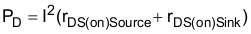
8.2.2.2 Slow-Decay SR (Brake Mode)
In slow-decay mode, both low-side sinking drivers turn on, allowing the current to circulate through the low side of the H-bridge (two sink drivers) and the load. Power dissipation I2R loses in the two sink DMOS drivers as shown in Equation 3.
Equation 3. 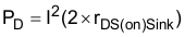
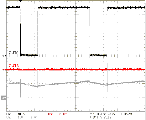
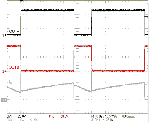
8.2.3 Application Curves