SLVSCI2A June 2014 – June 2014 DRV8802-Q1
PRODUCTION DATA.
- 1 Features
- 2 Applications
- 3 Description
- 4 Revision History
- 5 Pin Configuration and Functions
- 6 Specifications
- 7 Detailed Description
- 8 Application and Implementation
- 9 Power Supply Recommendations
- 10Layout
- 11Device and Documentation Support
- 12Mechanical, Packaging, and Orderable Information
Package Options
Mechanical Data (Package|Pins)
- PWP|28
Thermal pad, mechanical data (Package|Pins)
- PWP|28
Orderable Information
6 Specifications
6.1 Absolute Maximum Ratings
over operating free-air temperature range (unless otherwise noted)(1)(2)| MIN | MAX | UNIT | |||
|---|---|---|---|---|---|
| Power supply voltage | V(VMx) | –0.3 | 47 | V | |
| Charge pump voltage | VCP, CP1, CP2 | –0.3 | V(VMx)+7 | V | |
| Digital pin voltage | xPHASE, xENBL, nSLEEP, nFAULT, nRESET, xI0, xI1, DECAY | –0.5 | 7 | V | |
| Reference input voltage | V(xVREF) | –0.3 | 4 | V | |
| Sense pin voltage | V(ISENx) | –0.3 | 0.8 | V | |
| H-bridge output Current | xOUT1, xOUT2, ISENx | Peak motor drive, t < 1 μS | Internally limited | A | |
| Continuous motor drive(3) | 1.6 | A | |||
| Continuous total power dissipation | See the Power Dissipation section | ||||
| Operating virtual junction temperature, TJ | –40 | 150 | °C | ||
| Operating ambient temperature, TA | –40 | 125 | °C | ||
(1) Stresses beyond those listed under absolute maximum ratings may cause permanent damage to the device. These are stress ratings only, and functional operation of the device at these or any other conditions beyond those indicated under recommended operating conditions is not implied. Exposure to absolute–maximum–rated conditions for extended periods may affect device reliability.
(2) All voltage values are with respect to network ground terminal.
(3) Power dissipation and thermal limits must be observed.
6.2 Handling Ratings
| MIN | MAX | UNIT | ||||
|---|---|---|---|---|---|---|
| Tstg | Storage temperature range | –60 | 150 | °C | ||
| V(ESD) | Electrostatic discharge | Human body model (HBM), per AEC Q100-002(1) | –2000 | 2000 | V | |
| Charged device model (CDM), per AEC Q100-011 | Corner pins (1, 14, 15, and 28) | –750 | 750 | |||
| Other pins | –500 | 500 | ||||
(1) AEC Q100-002 indicates HBM stressing is done in accordance with the ANSI/ESDA/JEDEC JS-001 specification.
6.3 Recommended Operating Conditions
| MIN | MAX | UNIT | ||
|---|---|---|---|---|
| V(VMx) | Power supply voltage(1) | 8.2 | 45 | V |
| V(xVREF) | VREF input voltage(2) | 1 | 3.5 | V |
| I(OUT1x, OUT2x) | H-Bridge Output Current | 1.6 | A | |
| IL(V3P3OUT) | V3P3OUT load current | 1 | mA | |
(1) All VMx pins must be connected to the same supply voltage.
(2) Operational at V(xVREF) between 0 V and 1 V, but accuracy is degraded.
6.4 Thermal Information
| THERMAL METRIC(1) | PWP | UNIT | |
|---|---|---|---|
| 28 PINS | |||
| RθJA | Junction-to-ambient thermal resistance | 38.9 | °C/W |
| RθJC(top) | Junction-to-case (top) thermal resistance | 23.3 | |
| RθJB | Junction-to-board thermal resistance | 21.2 | |
| ψJT | Junction-to-top characterization parameter | 0.8 | |
| ψJB | Junction-to-board characterization parameter | 20.9 | |
| RθJC(bot) | Junction-to-case (bottom) thermal resistance | 2.6 | |
(1) For more information about traditional and new thermal metrics, see the IC Package Thermal Metrics application report, SPRA953.
6.5 Electrical Characteristics
over operating free-air temp range of -40°C to 125°C (unless otherwise noted)| PARAMETER | TEST CONDITIONS | MIN | TYP | MAX | UNIT | |
|---|---|---|---|---|---|---|
| POWER SUPPLIES | ||||||
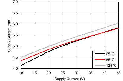
| I(VMx) | VMx operating supply current | V(VMx) = 24 V, ƒ(PWM) < 50 kHz | 5 | 8 | mA | |
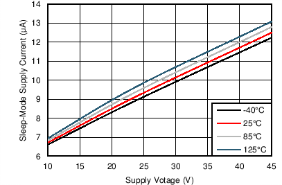
| I(VMx_Q) | VMx sleep mode supply current | V(VMx) = 24 V | 10 | 20 | μA | |
| V(UVLO) | VMx undervoltage lockout voltage | V(VMx) rising | 7.8 | 8.2 | V | |
| V3P3OUT REGULATOR | ||||||
| V(V3P3OUT) | V3P3OUT voltage | IO = 0 to 1 mA | 3.1 | 3.3 | 3.5 | V |
| LOGIC-LEVEL INPUTS | ||||||
| VIL | Input low voltage | 0.7 | V | |||
| VIH | Input high voltage | 2.1 | V | |||
| Vhys | Input hysteresis | 0.45 | V | |||
| IIL | Input low current | VI = 0 | –20 | 20 | μA | |
| IIH | Input high current | VI = 3.3 V | 100 | μA | ||
| nFAULT OUTPUT (OPEN-DRAIN OUTPUT) | ||||||
| VOL | Output low voltage | IO = 5 mA | 0.5 | V | ||
| IOH | Output high leakage current | VO = 3.3 V | 1 | μA | ||
| DECAY INPUT | ||||||
| VIL | Input low threshold voltage | For slow decay mode | 0 | 0.8 | V | |
| VIH | Input high threshold voltage | For fast decay mode | 2 | V | ||
| II | Input current | ±40 | µA | |||
| H-BRIDGE FETS | ||||||
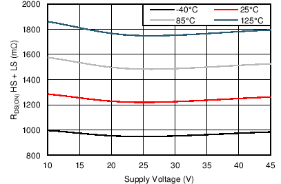
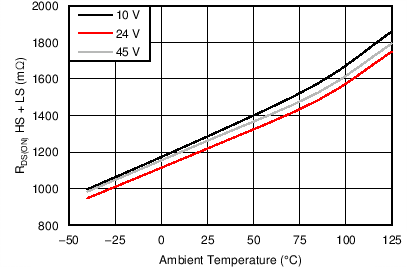
| rDS(on) | HS FET on resistance | VM = 24 V, IO = 1 A, TJ = 25°C | 0.63 | Ω | ||
| VM = 24 V, IO = 1 A, TJ = 85°C | 0.76 | 0.9 | ||||
| VM = 24 V, IO = 1 A, TJ = 125°C | 0.85 | 1 | ||||
| rDS(on) | LS FET on resistance | VM = 24 V, IO = 1 A, TJ = 25°C | 0.65 | Ω | ||
| VM = 24 V, IO = 1 A, TJ = 85°C | 0.78 | 0.9 | ||||
| VM = 24 V, IO = 1 A, TJ = 125°C | 0.85 | 1 | ||||
| Ilkg(OFF) | Off-state leakage current | –20 | 20 | μA | ||
| MOTOR DRIVER | ||||||
| ƒ(PWM) | Internal PWM frequency | 50 | kHz | |||
| t(blank) | Current-sense blanking time | 3.75 | μs | |||
| tr | Rise time | VM = 24 V | 100 | 360 | ns | |
| tf | Fall time | VM = 24 V | 80 | 250 | ns | |
| t(dead) | Dead time | 400 | ns | |||
| PROTECTION CIRCUITS | ||||||
| I(OCP) | Overcurrent protection trip level | 1.8 | 5 | A | ||
| T(SD) | Thermal shutdown temperature | Die temperature | 150 | 160 | 180 | °C |
| CURRENT CONTROL | ||||||
| I(xVREF) | xVREF input current | V(xVREF) = 3.3 V | –3 | 3 | μA | |
| V(TRIP) | xISENSE trip voltage | V(xVREF) = 3.3 V, 100% current setting | 635 | 660 | 685 | mV |
| V(xVREF) = 3.3 V, 71% current setting | 445 | 469 | 492 | |||
| V(xVREF) = 3.3 V, 38% current setting | 225 | 251 | 276 | |||
| G(ISENx) | Current sense amplifier gain | Reference only | 5 | V/V | ||
6.6 Typical Characteristics