SLRS063C September 2013 – February 2016 DRV8816
PRODUCTION DATA.
- 1 Features
- 2 Applications
- 3 Description
- 4 Revision History
- 5 Pin Configuration and Functions
- 6 Specifications
- 7 Detailed Description
- 8 Application and Implementation
- 9 Power Supply Recommendations
- 10Layout
- 11Device and Documentation Support
- 12Mechanical, Packaging, and Orderable Information
Package Options
Mechanical Data (Package|Pins)
- PWP|16
Thermal pad, mechanical data (Package|Pins)
- PWP|16
Orderable Information
8 Application and Implementation
NOTE
Information in the following applications sections is not part of the TI component specification, and TI does not warrant its accuracy or completeness. TI’s customers are responsible for determining suitability of components for their purposes. Customers should validate and test their design implementation to confirm system functionality.
8.1 Application Information
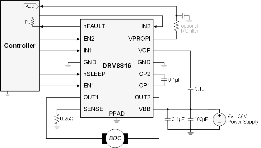
The DRV8816 is typically used to drive a brushed DC motor.
8.2 Typical Application
8.2.1 Design Requirements
Table 5 shows parameters to consider when designing.
Table 5. Design Parameters
| DESIGN PARAMETER | REFERENCE | EXAMPLE VALUE |
|---|---|---|
| Motor voltage | VBB | 24 V |
| Motor RMS current | IRMS | 0.8 A |
| Motor startup current | ISTART | 2 A |
| Motor current trip point | ITRIP | 2.5 A |
8.2.2 Detailed Design Procedure
8.2.2.1 Motor Voltage
The motor voltage to use will depend on the ratings of the motor selected and the desired RPM. A higher voltage spins a brushed DC motor faster with the same PWM duty cycle applied to the power FETs. A higher voltage also increases the rate of current change through the inductive motor windings.
8.2.2.2 Power Dissipation
The power dissipation of the DRV8816 is a function of RMS motor current and the each output’s FET resistance (RDS(ON)).

For this example, the ambient temperature is 35°C, and the junction temperature reaches 65°C. At 65°C, the sum of RDS(ON) is about 1Ω. With an example motor current of 0.8A, the dissipated power in the form of heat will be 0.8A² x 1Ω = 0.64W.
The temperature that the DRV8816 reaches will depend on the thermal resistance to the air and PCB. It is important to solder the device PowerPAD to the PCB ground plane, with vias to the top and bottom board layers, in order dissipate heat into the PCB and reduce the device temperature. In the example used here, the DRV8816 had an effective thermal resistance RθJA of 47°C/W, and:

8.2.2.3 Motor Current Trip Point
When the voltage on pin SENSE exceeds VTRIP (0.5V), overcurrent is detected. The RSENSE resistor should be sized to set the desired ITRIP level.

To set ITRIP to 2A, RSENSE = 0.5V / 2A = 0.25Ω.
To prevent false trips, ITRIP must be higher than regular operating current. Motor current during startup is typically much higher than steady-state spinning, because the initial load torque is higher, and the absence of back-EMF causes a higher voltage and extra current across the motor windings.
It can be beneficial to limit startup current by using series inductors on the DRV8816 output, as that allows ITRIP to be lower, and it may decrease the system’s required bulk capacitance. Startup current can also be limited by ramping the forward drive duty cycle.
8.2.2.4 Sense Resistor Selection
For optimal performance, it is important for the sense resistor to be:
- Surface-mount
- Low inductance
- Rated for high enough power
- Placed closely to the motor driver
The power dissipated by the sense resistor equals IRMS² x R. For example, if peak motor current is 3A, RMS motor current is 2A, and a 0.05Ω sense resistor is used, the resistor will dissipate 2A² x 0.05Ω = 0.2W. The power quickly increases with higher current levels.
Resistors typically have a rated power within some ambient temperature range, along with a de-rated power curve for high ambient temperatures. When a PCB is shared with other components generating heat, margin should be added. It is always best to measure the actual sense resistor temperature in a final system, along with the power MOSFETs, as those are often the hottest components.
Because power resistors are larger and more expensive than standard resistors, it is common practice to use multiple standard resistors in parallel, between the sense node and ground. This distributes the current and heat dissipation.
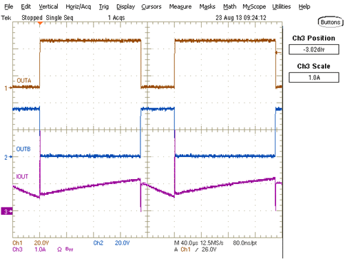
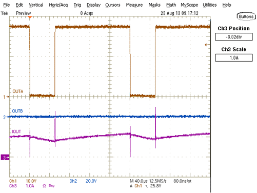
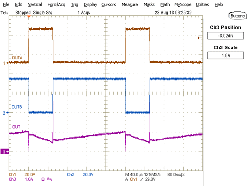
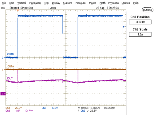
8.2.3 Application Curves
