SLVSCH4 July 2014 DRV8842-EP
PRODUCTION DATA.
- 1 Features
- 2 Applications
- 3 Description
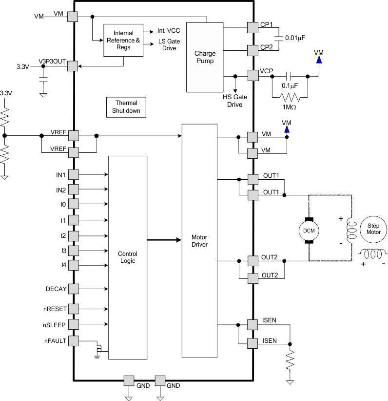
- 4 Simplified Schematic
- 5 Revision History
- 6 Pin Configuration and Functions
- 7 Specifications
- 8 Detailed Description
- 9 Application and Implementation
- 10Power Supply Recommendations
- 11Layout
- 12Device and Documentation Support
- 13Mechanical, Packaging, and Orderable Information
Package Options
Mechanical Data (Package|Pins)
- PWP|28
Thermal pad, mechanical data (Package|Pins)
- PWP|28
Orderable Information
8 Detailed Description
8.1 Overview
The DRV8842-EP provides an integrated motor driver solution for printers, scanners, and other automated equipment applications. The device has one H-bridge driver, and is intended to drive one DC motor, one coil of a stepper motor, or other loads. The output driver block consists of N-channel power MOSFETs configured as an H-bridge. The DRV8842-EP can supply up to 5-A peak or 3.5-A RMS output current (with proper heatsinking at 24 V and 25°C).
8.2 Functional Block Diagram
8.3 Feature Description
8.3.1 PWM Motor Drivers
The DRV8842-EP contains one H-bridge motor driver with current-control PWM circuitry. Figure 4 shows a block diagram of the motor control circuitry.
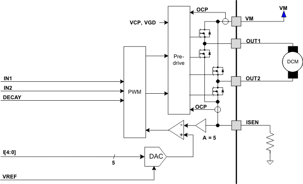 Figure 4. Motor Control Circuitry
Note that there are multiple VM, ISEN, OUT, and VREF pins. All like-named pins must be connected together on the PCB.
8.3.2 Bridge Control
The IN1 and IN2 input pins directly control the state of the OUT1 and OUT2 outputs. Either input can also be used for PWM control of the load. Table 1 shows the logic.
Table 1. H-Bridge Logic
| IN1 | IN2 | OUT1 | OUT2 |
|---|---|---|---|
| 0 | 0 | L | L |
| 0 | 1 | L | H |
| 1 | 0 | H | L |
| 1 | 1 | H | H |
The control inputs have internal pulldown resistors of approximately 100 kΩ.
8.3.3 Current Regulation
The maximum current through the load is regulated by a fixed-frequency PWM current regulation, or current chopping. When the H-bridge is enabled, current rises through the winding at a rate dependent on the DC voltage and inductance of the winding. After the current hits the current chopping threshold, the bridge disables the current until the beginning of the next PWM cycle.
For DC motors, current regulation is used to limit the start-up and stall current of the motor. Speed control is typically performed by providing an external PWM signal to the IN1 or IN2 input pins.
If the current regulation feature is not needed, it can be disabled by connecting the ISEN pins directly to ground and the VREF pins to V3P3.
The PWM chopping current is set by a comparator which compares the voltage across a current sense resistor connected to the ISEN pins, multiplied by a factor of 5, with a reference voltage. The reference voltage is input from the VREF pins, and is scaled by a 5-bit DAC that allows current settings of 0% to 100% in an approximately sinusoidal sequence.
The full-scale (100%) chopping current is calculated in Equation 1.
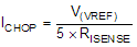
Example:
If using a 0.25-Ω sense resistor and the VREF pins are 2.5 V, the full-scale (100%) chopping current is 2.5 V / (5 × 0.25 Ω) = 2 A.
Five input pins (I0 through I4) are used to scale the current in the bridge as a percentage of the full-scale current set by the VREF input pin and sense resistance. The I0 through I4 pins have internal pulldown resistors of approximately 100 kΩ. The function of the pins is shown in Table 2.
Table 2. Pin Functions
| I[4..0] | RELATIVE CURRENT (% FULL-SCALE CHOPPING CURRENT) |
|---|---|
| 0x00h | 0% |
| 0x01h | 5% |
| 0x02h | 10% |
| 0x03h | 15% |
| 0x04h | 20% |
| 0x05h | 24% |
| 0x06h | 29% |
| 0x07h | 34% |
| 0x08h | 38% |
| 0x09h | 43% |
| 0x0Ah | 47% |
| 0x0Bh | 51% |
| 0x0Ch | 56% |
| 0x0Dh | 60% |
| 0x0Eh | 63% |
| 0x0Fh | 67% |
| 0x10h | 71% |
| 0x11h | 74% |
| 0x12h | 77% |
| 0x13h | 80% |
| 0x14h | 83% |
| 0x15h | 86% |
| 0x16h | 88% |
| 0x17h | 90% |
| 0x18h | 92% |
| 0x19h | 94% |
| 0x1Ah | 96% |
| 0x1Bh | 97% |
| 0x1Ch | 98% |
| 0x1Dh | 99% |
| 0x1Eh | 100% |
| 0x1Fh | 100% |
8.3.4 Blanking Time
After the current is enabled in an H-bridge, the voltage on the ISEN pin is ignored for a fixed period of time before enabling the current sense circuitry. This blanking time is fixed at 3.75 μs. Note that the blanking time also sets the minimum on-time of the PWM.
8.3.5 nRESET and nSLEEP Operation
The nRESET pin, when driven active low, resets the internal logic. It also disables the H-bridge driver. All inputs are ignored while nRESET is active.
Driving nSLEEP low puts the device into a low-power sleep state. In this state, the H-bridges are disabled, the gate drive charge pump is stopped, the V3P3OUT regulator is disabled, and all internal clocks are stopped. In this state, all inputs are ignored until nSLEEP returns inactive high. When returning from sleep mode, some time (approximately 1 ms) needs to pass before the motor driver becomes fully operational. Note that nRESET and nSLEEP have internal pulldown resistors of approximately 100 kΩ. These signals need to be driven to logic high for device operation.
8.3.6 Protection Circuits
The DRV8842-EP is fully protected against undervoltage, overcurrent, and overtemperature events.
8.3.6.1 Overcurrent Protection (OCP)
An analog current limit circuit on each FET limits the current through the FET by removing the gate drive. If this analog current limit persists for longer than the OCP time, all FETs in the H-bridge are disabled and the nFAULT pin is driven low. The device remains disabled until either nRESET pin is applied, or VM is removed and reapplied.
Overcurrent conditions on both high-side and low-side devices (that is, a short to ground, supply, or across the motor winding) all result in an overcurrent shutdown. Note that overcurrent protection does not use the current sense circuitry used for PWM current control, and is independent of the ISENSE resistor value or VREF voltage.
8.3.6.2 Thermal Shutdown (TSD)
If the die temperature exceeds safe limits, all FETs in the H-bridge are disabled and the nFAULT pin is driven low. After the die temperature has fallen to a safe level, operation automatically resumes.
8.3.6.3 Undervoltage Lockout (UVLO)
If at any time the voltage on the VM pins falls below the UVLO threshold voltage, all circuitry in the device is disabled and internal logic is reset. Operation resumes when VM rises above the UVLO threshold.
8.3.7 Thermal Protection
The DRV8842-EP has TSD as described in Thermal Shutdown (TSD). If the die temperature exceeds approximately 150°C, the device is disabled until the temperature drops to a safe level.
Any tendency of the device to enter TSD is an indication of either excessive power dissipation, insufficient heatsinking, or too high an ambient temperature.
8.3.8 Heatsinking
The PowerPAD™ package uses an exposed pad to remove heat from the device. For proper operation, this pad must be thermally connected to copper on the PCB to dissipate heat. On a multi-layer PCB with a ground plane, this can be accomplished by adding a number of vias to connect the thermal pad to the ground plane. On PCBs without internal planes, copper area can be added on either side of the PCB to dissipate heat. If the copper area is on the opposite side of the PCB from the device, thermal vias are used to transfer the heat between top and bottom layers.
For details about how to design the PCB, refer to TI application report SLMA002, PowerPAD™ Thermally Enhanced Package and TI application brief SLMA004, PowerPAD™ Made Easy, available at www.ti.com.
In general, the more copper area that can be provided, the more power can be dissipated.
8.4 Device Functional Modes
8.4.1 Decay Mode
During PWM current chopping, the H-bridge is enabled to drive current through the motor winding until it reaches the PWM current chopping threshold (see Figure 5, case 1). The current flow direction shown indicates the state when the IN1 pin is high and the IN2 pin is low.
After the chopping current threshold is reached, the H-bridge can operate in two different states, fast decay or slow decay.
In fast decay mode, after the PWM chopping current level is reached, the H-bridge reverses state to allow winding current to flow in a reverse direction. As the winding current approaches 0, the bridge is disabled to prevent any reverse current flow. Figure 5 case 2 shows fast decay mode.
In slow decay mode, winding current is recirculated by enabling both of the low-side FETs in the bridge (see Figure 5, case 3).
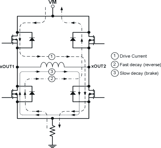 Figure 5. Decay Mode
The DRV8842-EP supports fast decay, slow decay, and a mixed decay mode. Slow, fast, or mixed decay mode is selected by the state of the DECAY pin. Logic low selects slow decay. Open selects mixed decay operation. And, logic high sets fast decay mode. The DECAY pin has both an internal pullup resistor of approximately 130 kΩ and an internal pulldown resistor of approximately 80 kΩ. This sets the mixed decay mode if the pin is left open or undriven.
Mixed decay mode begins as fast decay, but at a fixed period of time (75% of the PWM cycle) switches to slow decay mode for the remainder of the fixed PWM period.