SLVSCH4 July 2014 DRV8842-EP
PRODUCTION DATA.
- 1 Features
- 2 Applications
- 3 Description
- 4 Simplified Schematic
- 5 Revision History
- 6 Pin Configuration and Functions
- 7 Specifications
- 8 Detailed Description
- 9 Application and Implementation
- 10Power Supply Recommendations
- 11Layout
- 12Device and Documentation Support
- 13Mechanical, Packaging, and Orderable Information
Package Options
Mechanical Data (Package|Pins)
- PWP|28
Thermal pad, mechanical data (Package|Pins)
- PWP|28
Orderable Information
6 Pin Configuration and Functions
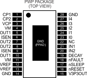
Pin Functions
| PIN | I/O(1) | DESCRIPTION | EXTERNAL COMPONENTS OR CONNECTIONS | |
|---|---|---|---|---|
| NAME | NO. | |||
| POWER AND GROUND | ||||
| GND | 14 | — | Device ground | |
| 28 | ||||
| VM | 4 | — | Bridge A power supply | Connect to motor supply (8.2 to 45 V). Both pins must be connected to same supply. |
| 11 | ||||
| V3P3OUT | 15 | O | 3.3-V regulator output | Bypass to GND with a 0.47-μF, 6.3-V ceramic capacitor. Can be used to supply VREF. |
| CP1 | 1 | IO | Charge pump flying capacitor | Connect a 0.01-μF 50-V capacitor between CP1 and CP2. |
| CP2 | 2 | IO | Charge pump flying capacitor | |
| VCP | 3 | IO | High-side gate drive voltage | Connect a 0.1-μF 16-V ceramic capacitor and a 1-MΩ resistor to VM. |
| CONTROL | ||||
| IN1 | 21 | I | Input 1 | Logic input controls state of OUT1. Internal pulldown. |
| IN2 | 20 | I | Input 2 | Logic input controls state of OUT2. Internal pulldown. |
| I0 | 23 | I | Current set inputs | Sets winding current as a percentage of full-scale. Internal pulldown. |
| I1 | 24 | I | ||
| I2 | 25 | I | ||
| I3 | 26 | I | ||
| I4 | 27 | I | ||
| DECAY | 19 | I | Decay mode | Low = slow decay, open = mixed decay, High = fast decay. Internal pulldown and pullup. |
| nRESET | 16 | I | Reset input | Active-low reset input initializes the logic and disables the H-bridge outputs. Internal pulldown. |
| nSLEEP | 17 | I | Sleep mode input | Logic high to enable device, logic low to enter low-power sleep mode. Internal pulldown. |
| VREF | 12 | I | Current set reference input | Reference voltage for winding current set. Both pins must be connected together on the PCB. |
| 13 | ||||
| STATUS | ||||
| nFAULT | 18 | OD | Fault | Logic low when in fault condition (over-temperature, overcurrent) |
| OUTPUT | ||||
| ISEN | 6 | IO | Bridge ground / Isense | Connect to current sense resistor. Both pins must be connected together on the PCB. |
| 9 | ||||
| OUT1 | 5 | O | Bridge output 1 | Connect to motor winding. Both pins must be connected together on the PCB. |
| 10 | ||||
| OUT2 | 7 | O | Bridge output 2 | Connect to motor winding. Both pins must be connected together on the PCB. |
| 8 | ||||
(1) Directions: I = input, O = output, OZ = tri-state output, OD = open-drain output, IO = input/output