SLVSFE6A August   2019  – April 2021 DRV8876N

PRODUCTION DATA  

  1. Features
  2. Applications
  3. Description
  4. Revision History
  5. Pin Configuration and Functions
    1.     Pin Functions
  6. Specifications
    1. 6.1 Absolute Maximum Ratings
    2. 6.2 ESD Ratings
    3. 6.3 Recommended Operating Conditions
    4. 6.4 Thermal Information
    5. 6.5 Electrical Characteristics
    6. 6.6 Typical Characteristics
  7. Detailed Description
    1. 7.1 Overview
    2. 7.2 Functional Block Diagram
    3. 7.3 Feature Description
      1. 7.3.1 External Components
      2. 7.3.2 Control Modes
        1. 7.3.2.1 PH/EN Control Mode (PMODE = Logic Low)
        2. 7.3.2.2 PWM Control Mode (PMODE = Logic High)
        3. 7.3.2.3 Independent Half-Bridge Control Mode (PMODE = Hi-Z)
      3. 7.3.3 Protection Circuits
        1. 7.3.3.1 VM Supply Undervoltage Lockout (UVLO)
        2. 7.3.3.2 VCP Charge Pump Undervoltage Lockout (CPUV)
        3. 7.3.3.3 OUTx Overcurrent Protection (OCP)
        4. 7.3.3.4 Thermal Shutdown (TSD)
        5. 7.3.3.5 Fault Condition Summary
      4. 7.3.4 Pin Diagrams
        1. 7.3.4.1 Logic-Level Inputs
        2. 7.3.4.2 Tri-Level Inputs
        3. 7.3.4.3 Quad-Level Inputs
    4. 7.4 Device Functional Modes
      1. 7.4.1 Active Mode
      2. 7.4.2 Low-Power Sleep Mode
      3. 7.4.3 Fault Mode
  8. Application and Implementation
    1. 8.1 Application Information
    2. 8.2 Typical Application
      1. 8.2.1 Primary Application
        1. 8.2.1.1 Design Requirements
        2. 8.2.1.2 Detailed Design Procedure
          1. 8.2.1.2.1 Power Dissipation and Output Current Capability
          2. 8.2.1.2.2 Thermal Performance
            1. 8.2.1.2.2.1 Steady-State Thermal Performance
            2. 8.2.1.2.2.2 Transient Thermal Performance
        3. 8.2.1.3 Application Curves
      2. 8.2.2 Alternative Application
        1. 8.2.2.1 Design Requirements
        2. 8.2.2.2 Detailed Design Procedure
        3. 8.2.2.3 Application Curves
  9. Power Supply Recommendations
    1. 9.1 Bulk Capacitance
  10. 10Layout
    1. 10.1 Layout Guidelines
    2. 10.2 Layout Example
      1. 10.2.1 HTSSOP Layout Example
  11. 11Device and Documentation Support
    1. 11.1 Documentation Support
      1. 11.1.1 Related Documentation
    2. 11.2 Receiving Notification of Documentation Updates
    3. 11.3 Community Resources
    4. 11.4 Trademarks
  12. 12Mechanical, Packaging, and Orderable Information

Package Options

Mechanical Data (Package|Pins)
Thermal pad, mechanical data (Package|Pins)
Orderable Information

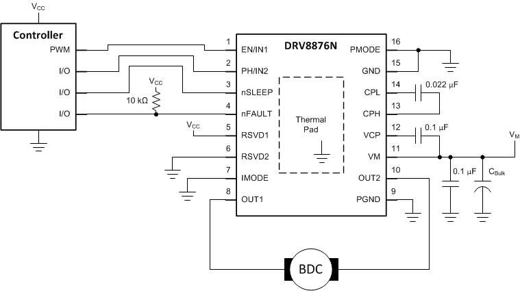
Primary Application

In the primary application example, the device is configured to drive a bidirectional current through an external load (such as a brushed DC motor) using an H-bridge configuration. The H-bridge polarity and duty cycle are controlled with a PWM and IO resource from the external controller to the EN/IN1 and PH/IN2 pins. The device is configured for the PH/EN control mode by tying the PMODE pin to GND.
GUID-2A83C34B-B89D-40D0-A32B-81D3D5150BCE-low.gifFigure 8-1 Typical Application Schematic