SLVSEE9D April 2020 – April 2021 DRV8889-Q1
PRODUCTION DATA
- 1 Features
- 2 Applications
- 3 Description
- 4 Revision History
- 5 Pin Configuration and Functions
- 6 Specifications
-
7 Detailed Description
- 7.1 Overview
- 7.2 Functional Block Diagram
- 7.3
Feature Description
- 7.3.1 Stepper Motor Driver Current Ratings
- 7.3.2 PWM Motor Drivers
- 7.3.3 Microstepping Indexer
- 7.3.4 Controlling VREF with an MCU DAC
- 7.3.5 Current Regulation
- 7.3.6
Decay Modes
- 7.3.6.1 Slow Decay for Increasing and Decreasing Current
- 7.3.6.2 Slow Decay for Increasing Current, Mixed Decay for Decreasing Current
- 7.3.6.3 Mode 4: Slow Decay for Increasing Current, Fast Decay for Decreasing current
- 7.3.6.4 Mixed Decay for Increasing and Decreasing Current
- 7.3.6.5 Smart tune Dynamic Decay
- 7.3.6.6 Smart tune Ripple Control
- 7.3.7 Blanking Time
- 7.3.8 Charge Pump
- 7.3.9 Linear Voltage Regulators
- 7.3.10 Logic Level Pin Diagrams
- 7.3.11 Protection Circuits
- 7.4 Device Functional Modes
- 7.5 Programming
- 7.6 Register Maps
-
8 Application and Implementation
- 8.1 Application Information
- 8.2 Typical Application
- 9 Power Supply Recommendations
- 10Layout
- 11Device and Documentation Support
- 12Mechanical, Packaging, and Orderable Information
Package Options
Mechanical Data (Package|Pins)
Thermal pad, mechanical data (Package|Pins)
Orderable Information
7.3.11.5 Stall Detection
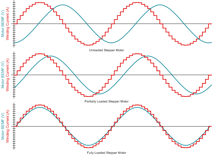
Stepper motors have a distinct relation between the winding current, back-EMF, and mechanical torque load of the motor, as shown in Figure 7-21. As motor load approaches the torque capability of the motor at a given winding current, the back-EMF will move in phase with the winding current. By detecting back-emf phase shift between rising and falling current quadrants of the motor current, the device can detect a motor overload stall condition or an end-of-line travel.
 Figure 7-21 Stall Detection by Monitoring Motor Back-EMF
The Stall Detection algorithm works only when the device is programmed to operate in the smart tune Ripple Control decay mode. The EN_STL bit in CTRL5 register has to be '1' to enable stall detection. The algorithm compares the back-EMF between the rising and falling current quadrants by monitoring PWM off time and generates a value represented by the 8-bit register TRQ_COUNT. The comparison is done in such a way that the TRQ_COUNT value is practically independent of motor current, motor winding resistance, ambient temperature and supply voltage. Full step mode of operation is supported by this algorithm.
For a lightly loaded motor, the TRQ_COUNT will be a non-zero value. As the motor approaches stall condition, TRQ_COUNT will approach zero and can be used to detect stall condition. If anytime TRQ_COUNT falls below the stall threshold (represented by the 8-bit STALL_TH register), device will detect stall and the STALL, STL and FAULT bits are latched high in the SPI register. To indicate stall detection fault on the nFAULT pin, the STL_REP bit in CTRL5 register has to be '1'. When the STL_REP bit is '1', the nFAULT pin will be driven low when stall is detected. In stalled condition, the motor shaft does not spin. The motor starts to spin again when the stall condition is removed. The nFAULT line is released and the fault registers are cleared when a clear faults command has been issued either through the CLR_FLT bit or an nSLEEP reset pulse.
TRQ_CNT gets calculated as an average from the latest four electrical half-cycles. Once calculated, it gets updated in the SPI register within 100 ns. After the latest TRQ_CNT is updated, it retains the value in the SPI register for the next electrical half-cycle, after which the TRQ_CNT is updated with a new value. The duration of the electrical half-cycle is dependent on microstepping and step-frequency. At the most, it takes two electrical cycles to detect stall.
Stall threshold can be set in two ways – either user can write the STALL_TH bits, or let the algorithm learn the stall threshold value itself through the stall learning process. The stall learning process requires that the STL_LRN bit in CTRL5 register is '1' and the motor is deliberately stalled for some time to allow the algorithm to learn the ideal stall threshold. The process takes 16 electrical cycles and at the end of a successful learning, loads the STALL_TH register with the proper stall threshold bits. Also, the STL_LRN_OK bit goes high at the end of successful learning. It is recommended that users set the stall threshold using the stall learning process for proper stall detection. A stall threshold at one speed may not work well for another speed - therefore it is recommended to re-learn the stall threshold when the motor speed changes.