SNLS399B January 2012 – January 2015 DS100DF410
PRODUCTION DATA.
- 1 Features
- 2 Applications
- 3 Description
- 4 Revision History
- 5 Pin Configuration and Functions
- 6 Specifications
-
7 Detailed Description
- 7.1 Overview
- 7.2 Functional Block Diagram
- 7.3
Feature Description
- 7.3.1 Device Data Path Operation
- 7.3.2 Signal Detect
- 7.3.3 CTLE
- 7.3.4 DFE
- 7.3.5 Clock and Data Recovery
- 7.3.6 Output Driver
- 7.3.7 CTLE Boost Setting
- 7.3.8 DFE Tap Weight and Polarity Setting
- 7.3.9 Driver Output Voltage
- 7.3.10 Driver Output De-Emphasis
- 7.3.11 Driver Output Rise/Fall Time
- 7.3.12 Ref_mode 0 Mode (Reference Clock Not Required)
- 7.3.13 Ref_mode 3 Mode (Reference Clock Required)
- 7.3.14 False Lock Detector Setting
- 7.3.15 Reference Clock In
- 7.3.16 Reference Clock Out
- 7.3.17 Daisy Chain of REFCLK_OUT to REFCLK_IN
- 7.3.18 INT
- 7.3.19 LOCK_3, LOCK_2, LOCK_1, and LOCK_0
- 7.4 Device Functional Modes
- 7.5
Programming
- 7.5.1 SMBus Strap Observation
- 7.5.2 Device Revision and Device ID
- 7.5.3 Control/Shared Register Reset
- 7.5.4 Interrupt Channel Flag Bits
- 7.5.5 SMBus Master Mode Control Bits
- 7.5.6 Resetting Individual Channels of the Retimer
- 7.5.7 Interrupt Status
- 7.5.8 Overriding the CTLE Boost Setting
- 7.5.9 Overriding the VCO CAP DAC Values
- 7.5.10 Overriding the Output Multiplexer
- 7.5.11 Overriding the VCO Divider Selection
- 7.5.12 Using the PRBS Generator
- 7.5.13 Using the Internal Eye Opening Monitor
- 7.5.14 Overriding the DFE Tap Weights and Polarities
- 7.5.15 Enabling Slow Rise/Fall Time on the Output Driver
- 7.5.16 Inverting the Output Polarity
- 7.5.17 Overriding the Figure of Merit for Adaptation
- 7.5.18 Setting the Rate and Subrate for Lock Acquisition
- 7.5.19 Setting the Adaptation/Lock Mode
- 7.5.20 Initiating Adaptation
- 7.5.21 Setting the Reference Enable Mode
- 7.5.22 Overriding the CTLE Settings Used for CTLE Adaptation
- 7.5.23 Setting the Output Differential Voltage
- 7.5.24 Setting the Output De-emphasis Setting
- 7.6 Register Maps
- 8 Application and Implementation
- 9 Power Supply Recommendations
- 10Layout
- 11Device and Documentation Support
- 12Mechanical, Packaging, and Orderable Information
Package Options
Mechanical Data (Package|Pins)
- RHS|48
Thermal pad, mechanical data (Package|Pins)
- RHS|48
Orderable Information
10 Layout
10.1 Layout Guidelines
The CML inputs and outputs have been optimized to work with interconnects using a controlled differential impedance of 100 Ω. It is preferable to route differential lines exclusively on one layer of the board, particularly for the input traces. The use of vias should be avoided if possible. If vias must be used, they should be used sparingly and must be placed symmetrically for each side of a given differential pair. Whenever differential vias are used the layout must also provide for a low inductance path for the return currents as well. Route the differential signals away from other signals and noise sources on the printed circuit board. See AN-1187 Leadless Leadframe Package (LLP) Application Report (SNOA401) for additional information on QFN (WQFN) packages.
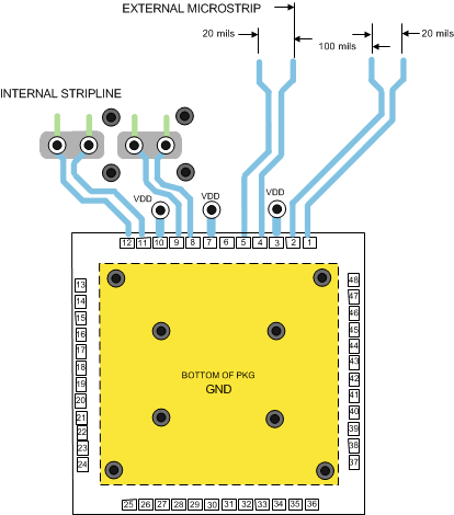
10.2 Layout Example
To minimize the effects of crosstalk, a 5:1 ratio or greater should be maintained between inter-pair spacing.
Figure 10 depicts different transmission line topologies which can be used in various combinations to achieve the optimal system performance. Impedance discontinuities at the differential via can be minimized or eliminated by increasing the swell around each hole and providing for a low inductance return current path. When the via structure is associated with thick backplane PCB, further optimization such as back drilling is often used to reduce the detrimental high frequency effects of stubs on the signal path.