SNLS542C October 2016 – December 2020 DS280MB810
PRODUCTION DATA
- 1 Features
- 2 Applications
- 3 Description
- 4 Revision History
- 5 Description (continued)
- 6 Pin Configuration and Functions
- 7 Specifications
- 8 Detailed Description
- 9 Application and Implementation
- 10Power Supply Recommendations
- 11Layout
- 12Device and Documentation Support
- 13Mechanical, Packaging, and Orderable Information
Package Options
Mechanical Data (Package|Pins)
- ZBL|135
Thermal pad, mechanical data (Package|Pins)
Orderable Information
3 Description
The DS280MB810 is an extremely low-power, high-performance eight-channel linear equalizer supporting multi-rate, multi-protocol interfaces up to 28 Gbaud NRZ. It is used to extend the reach and improve the robustness of high-speed serial links for backplane, front-port, and chip-to-chip applications.
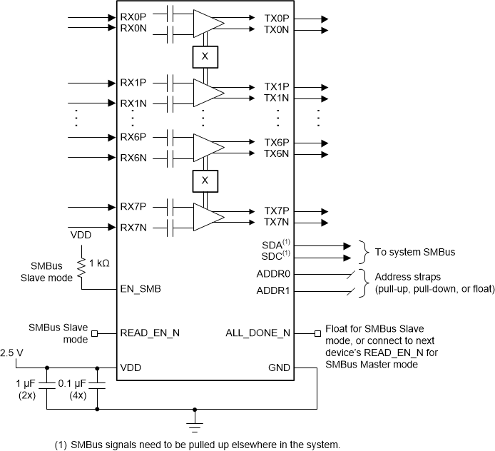
The DS280MB810 includes a full 2x2 cross-point switch between each pair of adjacent channels which enables 2-to-1 multiplexing and 1-to-2 de-multiplexing applications for failover redundancy, as well as signal cross-over to aid PCB routing. The cross-point can be controlled through pins or the SMBus register interface.
The linear nature of the DS280MB810’s equalization preserves the transmit signal characteristics, thereby allowing the host and link partner ASICs to freely negotiate transmit equalizer coefficients (100G-CR4/KR4). This transparency to the link training protocol facilitates system-level interoperability with minimal effect on the latency. The DS280MB810 supports two-level pulse amplitude modulation (PAM), or NRZ, for symbol rates up to 28 Gbaud and peak signal amplitude within the linear operating range.
Each channel operates independently, and every channel can be configured uniquely. In most application scenarios, the same configuration can be used regardless of data rate.
The DS280MB810's small package dimensions, optimized high-speed signal escape, and the pin-compatible Retimer portfolio make the DS280MB810 ideal for high-density backplane applications. Simplified equalization control, low power consumption, and ultra-low additive jitter make it suitable for front-port interfaces such as 100G-SR4/LR4/CR4. The small 8-mm x 13-mm footprint easily fits behind numerous standard front-port connectors like QSFP, SFP, CFP, and CDFP without the need for a heat sink.
| PART NUMBER | PACKAGE | BODY SIZE (NOM) |
|---|---|---|
| DS280MB810 | nFBGA(135) | 8.0 mm x 13.0 mm |
 Simplified Schematic