SNLS542C October   2016  – December 2020 DS280MB810

PRODUCTION DATA  

  1. Features
  2. Applications
  3. Description
  4. Revision History
  5. Description (continued)
  6. Pin Configuration and Functions
  7. Specifications
    1. 7.1 Absolute Maximum Ratings
    2. 7.2 ESD Ratings
    3. 7.3 Recommended Operating Conditions
    4. 7.4 Thermal Information
    5. 7.5 Electrical Characteristics
    6. 7.6 Timing Requirements – Serial Management Bus Interface
    7. 7.7 Typical Characteristics
  8. Detailed Description
    1. 8.1 Overview
    2. 8.2 Functional Block Diagram
    3. 8.3 Feature Description
      1. 8.3.1 Device Data Path Operation
      2. 8.3.2 AC-coupled Receiver Inputs
      3. 8.3.3 Signal Detect
      4. 8.3.4 2-Stage CTLE
      5. 8.3.5 Driver DC Gain Control
      6. 8.3.6 2x2 Cross-point Switch
      7. 8.3.7 Configurable SMBus Address
    4. 8.4 Device Functional Modes
      1. 8.4.1 SMBus Slave Mode Configuration
      2. 8.4.2 SMBus Master Mode Configuration (EEPROM Self Load)
    5. 8.5 Programming
      1. 8.5.1 Transfer of Data with the SMBus Interface
    6. 8.6 Register Maps
      1. 8.6.1 Register Types: Global, Shared, and Channel
      2. 8.6.2 Global Registers: Channel Selection and ID Information
      3. 8.6.3 Shared Registers
      4. 8.6.4 Channel Registers
  9. Application and Implementation
    1. 9.1 Application Information
    2. 9.2 Typical Application
      1. 9.2.1 Backplane and Mid-Plane Reach Extension
        1. 9.2.1.1 Design Requirements
        2. 9.2.1.2 Detailed Design Procedure
      2. 9.2.2 Front-Port Applications
        1. 9.2.2.1 Design Requirements
        2. 9.2.2.2 Detailed Design Procedure
      3. 9.2.3 Application Curves
        1. 9.2.3.1 Pattern Generator Characteristics
        2. 9.2.3.2 Equalizing Moderate Pre-Channel Loss
        3. 9.2.3.3 Equalizing High Pre-Channel Loss
        4. 9.2.3.4 Equalizing High Pre-Channel Loss and Moderate Post-Channel Loss
    3. 9.3 Initialization Set Up
  10. 10Power Supply Recommendations
  11. 11Layout
    1. 11.1 Layout Guidelines
    2. 11.2 Layout Examples
      1. 11.2.1 Stripline Example
      2. 11.2.2 Microstrip Example
  12. 12Device and Documentation Support
    1. 12.1 Documentation Support
      1. 12.1.1 Related Documentation
    2. 12.2 Receiving Notification of Documentation Updates
    3. 12.3 Support Resources
    4. 12.4 Trademarks
  13. 13Mechanical, Packaging, and Orderable Information

Package Options

Mechanical Data (Package|Pins)
Thermal pad, mechanical data (Package|Pins)
Orderable Information

Pattern Generator Characteristics

All of the example application results in the sections which follow were tested using a pattern generator with the following characteristics.

GUID-3D30A76D-7911-456B-8E11-3556AEFF52C7-low.gifFigure 9-10 Pattern Generator test setup
GUID-1B8A8FBB-212F-4ED7-B6E9-5C03ABA9ADE8-low.pngFigure 9-11 Pattern Generator output at 25.78125 Gbps, 800m Vppd, PRBS9
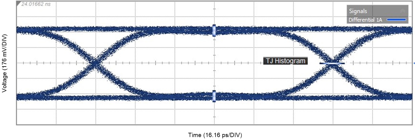
GUID-5232D9E1-DA1B-4020-894C-8AADDBF705DD-low.pngFigure 9-12 Pattern Generator output at 10.31250 Gbps, 800 mVppd, PRBS9
Table 9-1 Pattern Generator Characteristics
25.78125 Gbps10.3125 Gbps
Differential peak-to-peak voltage (VOD)~800 mVppd~800 mVppd
Channel loss between Pattern Generator and Scope2 dB @ 12.9 GHz1 dB @ 5.2 GHz
Total Jitter @ 1E-158.0 psP-P13.4 psP-P
Differential Eye Height @ 1E-15448 mVP-P596 mVP-P