SNLS206B September   2005  – January 2019 DS90LV027AH

PRODUCTION DATA.  

  1. Features
  2. Applications
  3. Description
    1.     Device Images
      1.      Functional Diagram of Channel 1
      2.      Functional Diagram of Channel 2
  4. Revision History
  5. Pin Configuration and Functions
    1.     Pin Functions
  6. Specifications
    1. 6.1 Absolute Maximum Ratings
    2. 6.2 ESD Ratings
    3. 6.3 Recommended Operating Conditions
    4. 6.4 Thermal Information
    5. 6.5 Electrical Characteristics
    6. 6.6 Switching Characteristics
    7. 6.7 Typical Characteristics
  7. Parameter Measurement Information
  8. Detailed Description
    1. 8.1 Overview
    2. 8.2 Functional Block Diagrams
    3. 8.3 Feature Description
      1. 8.3.1 DS90LV027AH Driver Functionality
      2. 8.3.2 Driver Output Voltage and Power-On Reset
      3. 8.3.3 Driver Offset
    4. 8.4 Device Functional Modes
  9. Application and Implementation
    1. 9.1 Application Information
    2. 9.2 Typical Application
      1. 9.2.1 Design Requirements
      2. 9.2.2 Detailed Design Procedure
        1. 9.2.2.1 Driver Supply Voltage
        2. 9.2.2.2 Driver Bypass Capacitance
        3. 9.2.2.3 Driver Input Votlage
        4. 9.2.2.4 Driver Output Voltage
        5. 9.2.2.5 Interconnecting Media
        6. 9.2.2.6 PCB Transmission Lines
      3. 9.2.3 Termination Resistor
      4. 9.2.4 Application Curve
  10. 10Power Supply Recommendations
  11. 11Layout
    1. 11.1 Layout Guidelines
      1. 11.1.1 Microstrip vs. Stripline Topologies
      2. 11.1.2 Dielectric Type and Board Construction
      3. 11.1.3 Recommended Stack Layout
      4. 11.1.4 Separation Between Traces
      5. 11.1.5 Crosstalk and Ground Bounce Minimization
      6. 11.1.6 Decoupling
    2. 11.2 Layout Example
  12. 12Device and Documentation Support
    1. 12.1 Related Documentation
    2. 12.2 Receiving Notification of Documentation Updates
    3. 12.3 Community Resources
    4. 12.4 Trademarks
    5. 12.5 Electrostatic Discharge Caution
    6. 12.6 Glossary
  13. 13Mechanical, Packaging, and Orderable Information

Package Options

Mechanical Data (Package|Pins)
Thermal pad, mechanical data (Package|Pins)
Orderable Information

Recommended Stack Layout

Following the choice of dielectrics and design specifications, the designer must decide how many levels to use in the stack. To reduce the LVCMOS/LVTTL to LVDS crosstalk, it is good practice to have at least two separate signal planes as shown in Figure 26.

DS90LV027AH lo_4lpcbb_slls373.gifFigure 26. Four-Layer PCB

NOTE

The separation between layers 2 and 3 should be 127 μm (0.005 in). By keeping the power and ground planes tightly coupled, the increased capacitance acts as a bypass for transients.

One of the most common stack configurations is the six-layer board, as shown in Figure 27.
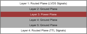
DS90LV027AH lo_6lpcbb_slls373.gifFigure 27. Six-Layer PCB

In this particular configuration, it is possible to isolate each signal layer from the power plane by at least one ground plane. The result is improved signal integrity, but fabrication is more expensive. Using the 6-layer board is preferable, because it offers the layout designer more flexibility in varying the distance between signal layers and referenced planes in addition to ensuring reference to a ground plane for signal layers 1 and 6.