SNLS336J October 2010 – November 2014 DS90UH925Q-Q1
PRODUCTION DATA.
- 1 Features
- 2 Applications
- 3 Description
- 4 Revision History
- 5 Pin Configuration and Functions
-
6 Specifications
- 6.1 Absolute Maximum Ratings
- 6.2 Handling Ratings
- 6.3 Recommended Operating Conditions
- 6.4 Thermal Information
- 6.5 DC Electrical Characteristics
- 6.6 AC Electrical Characteristics
- 6.7 DC and AC Serial Control Bus Characteristics
- 6.8 Recommended Timing for Serial Control Bus
- 6.9 Switching Characteristics
- 6.10 Typical Charateristics
-
7 Detailed Description
- 7.1 Overview
- 7.2 Functional Block Diagram
- 7.3
Feature Description
- 7.3.1 High Speed Forward Channel Data Transfer
- 7.3.2 Low Speed Back Channel Data Transfer
- 7.3.3 Backward Compatible Mode
- 7.3.4 Common Mode Filter Pin (CMF)
- 7.3.5 Video Control Signal Filter
- 7.3.6 Power Down (PDB)
- 7.3.7 Remote Auto Power Down Mode
- 7.3.8 LVCMOS VDDIO Option
- 7.3.9 Input PCLK Loss Detect
- 7.3.10 Serial Link Fault Detect
- 7.3.11 Pixel Clock Edge Select (RFB)
- 7.3.12 Low Frequency Optimization (LFMODE)
- 7.3.13 Interrupt Pin — Functional Description and Usage (INTB)
- 7.3.14 EMI Reduction Features
- 7.4 Device Functional Modes
- 7.5 Programming
- 7.6 Register Maps
- 8 Applications and Implementation
- 9 Power Supply Recommendations
- 10Layout
- 11Device and Documentation Support
- 12Mechanical, Packaging, and Orderable Information
Package Options
Mechanical Data (Package|Pins)
- RHS|48
Thermal pad, mechanical data (Package|Pins)
- RHS|48
Orderable Information
6 Specifications
6.1 Absolute Maximum Ratings (1)(2)
over operating free-air temperature range (unless otherwise noted)| MIN | MAX | UNIT | ||
|---|---|---|---|---|
| Supply Voltage – VDD33 | -0.3 | 4.0 | V | |
| Supply Voltage – VDDIO | -0.3 | 4.0 | V | |
| LVCMOS I/O Voltage(3) | -0.3 | VDDIO + 0.3 | V | |
| Serializer Output Voltage | -0.3 | 2.75 | V | |
| Junction Temperature | 150 | °C | ||
(1) If Military/Aerospace specified devices are required, please contact the Texas Instruments Sales Office/ Distributors for availability and specifications.
(2) “Absolute Maximum Ratings” indicate limits beyond which damage to the device may occur, including inoperability and degradation of device reliability and/or performance. Functional operation of the device and/or non-degradation at the Absolute Maximum Ratings or other conditions beyond those indicated in the Recommended Operating Conditions is not implied. The Recommended Operating Conditions indicate conditions at which the device is functional and the device should not be operated beyond such conditions.
(3) The maximum limit (VDDIO +0.3V) does not apply to the PDB pin during the transition to the power down state (PDB transitioning from HIGH to LOW).
6.2 Handling Ratings
| MIN | MAX | UNIT | ||||
|---|---|---|---|---|---|---|
| Tstg | Storage temperature range | -65 | +150 | °C | ||
| V(ESD) | Electrostatic discharge | Human body model (HBM), per AEC Q100-002(1) | ±8 | ±8 | kV | |
| Charged device model (CDM), per AEC Q100-011 | ±1.25 | ±1.25 | ||||
| Machine Model (MM) | ±250 | ±250 | V | |||
| ESD Rating (IEC 61000-4-2, powered-up only) RD= 330Ω, CS = 150pF |
Air Discharge (DOUT+, DOUT-) |
±15 | ±15 | kV | ||
| Contact Discharge (DOUT+, DOUT-) |
±8 | ±8 | ||||
| ESD Rating (ISO 10605) RD= 330Ω, CS = 150pF/330pF RD= 2KΩ, CS = 150pF/330pF |
Air Discharge (DOUT+, DOUT-) |
±15 | ±15 | |||
| Contact Discharge (DOUT+, DOUT-) |
±8 | ±8 | ||||
(1) AEC Q100-002 indicates HBM stressing is done in accordance with the ANSI/ESDA/JEDEC JS-001 specification.
6.3 Recommended Operating Conditions
over operating free-air temperature range (unless otherwise noted)| MIN | NOM | MAX | UNIT | |
|---|---|---|---|---|
| Supply Voltage (VDD33) | 3.0 | 3.3 | 3.6 | V |
| LVCMOS Supply Voltage (VDDIO) | 3.0 | 3.3 | 3.6 | V |
| OR | ||||
| LVCMOS Supply Voltage (VDDIO) | 1.71 | 1.8 | 1.89 | V |
| Operating Free Air Temperature (TA) | −40 | 25 | 105 | °C |
| PCLK Frequency | 5 | 85 | MHz | |
| Supply Noise | 100 | mVP-P |
6.4 Thermal Information
| THERMAL METRIC(1) | RHS | UNIT | |
|---|---|---|---|
| 48 PINS | |||
| RθJA | Junction-to-ambient thermal resistance | 35 | °C/W |
| RθJC(top) | Junction-to-case (top) thermal resistance | 5.2 | |
| RθJB | Junction-to-board thermal resistance | 5.5 | |
| ψJT | Junction-to-top characterization parameter | 0.1 | |
| ψJB | Junction-to-board characterization parameter | 5.5 | |
| RθJC(bot) | Junction-to-case (bottom) thermal resistance | 1.3 | |
(1) For more information about traditional and new thermal metrics, see the IC Package Thermal Metrics application report, SPRA953.
6.5 DC Electrical Characteristics(1)(2)(3)
Over recommended operating supply and temperature ranges unless otherwise specified.| PARAMETER | TEST CONDITIONS | PIN/FREQ. | MIN | TYP | MAX | UNIT | ||
|---|---|---|---|---|---|---|---|---|
| LVCMOS I/O DC SPECIFICATIONS | ||||||||
| VIH | High Level Input Voltage | VDDIO = 3.0 to 3.6V | PDB | 2.0 | VDDIO | V | ||
| VIL | Low Level Input Voltage | VDDIO = 3.0 to 3.6V | GND | 0.8 | V | |||
| IIN | Input Current | VIN = 0V or VDDIO = 3.0 to 3.6V | −10 | ±1 | 10 | μA | ||
| VIH | High Level Input Voltage | VDDIO = 3.0 to 3.6V | R[7:0], G[7:0], B[7:0], HS, VS, DE, PCLK, I2S_CLK, I2S_WC, I2S_DA, I2S_DB | 2.0 | VDDIO | V | ||
| VDDIO = 1.71 to 1.89V | 0.65* VDDIO |
VDDIO | V | |||||
| VIL | Low Level Input Voltage | VDDIO = 3.0 to 3.6V | GND | 0.8 | V | |||
| VDDIO = 1.71 to 1.89V | GND | 0.35* VDDIO |
V | |||||
| IIN | Input Current | VIN = 0V or VDDIO | VDDIO = 3.0 to 3.6V |
−10 | ±1 | 10 | μA | |
| VDDIO = 1.71 to 1.89V |
−10 | ±1 | 10 | μA | ||||
| VOH | High Level Output Voltage | IOH = −4mA | VDDIO = 3.0 to 3.6V | GPIO[3:0], GPO_REG[8:4] | 2.4 | VDDIO | V | |
| VDDIO = 1.71 to 1.89V |
VDDIO - 0.45 | VDDIO | V | |||||
| VOL | Low Level Output Voltage | IOL = +4mA | VDDIO = 3.0 to 3.6V | GND | 0.4 | V | ||
| VDDIO = 1.71 to 1.89V |
GND | 0.35 | V | |||||
| IOS | Output Short Circuit Current | VOUT = 0V | −50 | mA | ||||
| IOZ | TRI-STATE® Output Current | VOUT = 0V or VDDIO, PDB = L, | −10 | 10 | μA | |||
| FPD-LINK III CML DRIVER DC SPECIFICATIONS | ||||||||
| VODp-p | Differential Output Voltage (DOUT+) – (DOUT-) |
RL = 100Ω, Figure 1 | DOUT+, DOUT- | 1160 | 1250 | 1340 | mVp-p | |
| ΔVOD | Output Voltage Unbalance | 1 | 50 | mV | ||||
| VOS | Offset Voltage – Single-ended | RL = 100Ω, Figure 1 | 2.5-0.25*VODp-p (TYP) | V | ||||
| ΔVOS | Offset Voltage Unbalance Single-ended |
1 | 50 | mV | ||||
| IOS | Output Short Circuit Current | DOUT+/- = 0V, PDB = L or H |
−38 | mA | ||||
| RT | Internal Termination Resistor - Single ended | 40 | 52 | 62 | Ω | |||
| SUPPLY CURRENT | ||||||||
| IDD1 | Supply Current (includes load current) RL = 100Ω, f = 85 MHz |
Checker Board Pattern, Figure 2 |
VDD33= 3.6V | VDD33 | 148 | 170 | mA | |
| IDDIO1 | VDDIO = 3.6V | VDDIO | 90 | 180 | μA | |||
| VDDIO = 1.89V | 1 | 1.6 | mA | |||||
| IDDS1 | Supply Current Remote Auto Power Down Mode | 0x01[7] = 1, deserializer is powered down | VDD33 = 3.6V | VDD33 | 1.2 | 2.4 | mA | |
| IDDIOS1 | VDDIO = 3.6V | VDDIO | 65 | 150 | μA | |||
| VDDIO = 1.89V | 55 | 150 | μA | |||||
| IDDS2 | Supply Current Power Down | PDB = L, All LVCMOS inputs are floating or tied to GND | VDD33 = 3.6V | VDD33 | 1 | 2 | mA | |
| IDDIOS2 | VDDIO = 3.6V | VDDIO | 65 | 150 | μA | |||
| VDDIO = 1.89V | 50 | 150 | μA | |||||
6.6 AC Electrical Characteristics
Over recommended operating supply and temperature ranges unless otherwise specified.(1)(2)(3)| PARAMETER | TEST CONDITIONS | PIN/FREQ. | MIN | TYP | MAX | UNIT | |
|---|---|---|---|---|---|---|---|
| GPIO BIT RATE | |||||||
| BR | Forward Channel Bit Rate | See(7)(4) | f = 5 – 85 MHz GPIO[3:0] |
0.25* f | Mbps | ||
| Back Channel Bit Rate | 75 | kbps | |||||
| RECOMMENDED TIMING for PCLK | |||||||
| tTCP | PCLK Period | See(7)(4) | PCLK | 11.76 | T | 200 | ns |
| tCIH | PCLK Input High Time | 0.4*T | 0.5*T | 0.6*T | ns | ||
| tCIL | PCLK Input Low Time | 0.4*T | 0.5*T | 0.6*T | ns | ||
| tCLKT | PCLK Input Transition Time Figure 3(7)(4) |
f = 5 MHz | 4.0 | ns | |||
| f = 85 MHz | 0.5 | ns | |||||
| tIJIT | PCLK Input Jitter Tolerance, Bit Error Rate ≤10–10 |
f / 40 < Jitter Freq < f / 20(4)(5) | f = 5 – 78MHz | 0.4 | 0.6 | UI | |
(1) The Electrical Characteristics tables list ensured specifications under the listed Recommended Operating Conditions except as otherwise modified or specified by the Electrical Characteristics Conditions and/or Notes. Typical specifications are estimations only and are not ensured.
(2) Typical values represent most likely parametric norms at VDD = 3.3 V, TA = +25 °C, and at the Recommended Operating Conditions at the time of product characterization and are not ensured.
(3) Current into device pins is defined as positive. Current out of a device pin is defined as negative. Voltages are referenced to ground except VOD and ΔVOD, which are differential voltages.
(4) Specification is ensured by characterization and is not tested in production.
(5) Jitter Frequency is specified in conjunction with DS90UH926 PLL bandwidth.
6.7 DC and AC Serial Control Bus Characteristics
Over 3.3V supply and temperature ranges unless otherwise specified.(1)(2)(3)| PARAMETER | TEST CONDITIONS | MIN | TYP | MAX | UNIT | |
|---|---|---|---|---|---|---|
| VIH | Input High Level | SDA and SCL | 0.7* VDD33 |
VDD33 | V | |
| VIL | Input Low Level Voltage | SDA and SCL | GND | 0.3* VDD33 |
V | |
| VHY | Input Hysteresis | >50 | mV | |||
| VOL | SDA, IOL = 1.25 mA | 0 | 0.36 | V | ||
| Iin | SDA or SCL, VIN = VDD33 or GND | -10 | 10 | µA | ||
| tR | SDA RiseTime – READ | SDA, RPU = 10 kΩ, Cb ≤ 400 pF, see Figure 8 | 430 | ns | ||
| tF | SDA Fall Time – READ | 20 | ns | |||
| tSU;DAT | Set Up Time — READ | See Figure 8 | 560 | ns | ||
| tHD;DAT | Hold Up Time — READ | See Figure 8 | 615 | ns | ||
| tSP | Input Filter | 50 | ns | |||
| Cin | Input Capacitance | SDA or SCL | <5 | pF | ||
(1) The Electrical Characteristics tables list ensured specifications under the listed Recommended Operating Conditions except as otherwise modified or specified by the Electrical Characteristics Conditions and/or Notes. Typical specifications are estimations only and are not ensured.
(2) Typical values represent most likely parametric norms at VDD = 3.3 V, TA = +25 °C, and at the Recommended Operating Conditions at the time of product characterization and are not ensured.
(3) Current into device pins is defined as positive. Current out of a device pin is defined as negative. Voltages are referenced to ground except VOD and ΔVOD, which are differential voltages.
(4) tPLD is the time required by the device to obtain lock when exiting power-down state with an active PCLK.
(5) UI – Unit Interval is equivalent to one serialized data bit width (1UI = 1 / 35*PCLK). The UI scales with PCLK frequency.
(6) Specification is ensured by characterization and is not tested in production.
(7) Specification is ensured by design and is not tested in production.
6.8 Recommended Timing for Serial Control Bus
Over 3.3V supply and temperature ranges unless otherwise specified.| MIN | TYP | MAX | UNITS | |||
|---|---|---|---|---|---|---|
| fSCL | SCL Clock Frequency | Standard Mode | 0 | 100 | kHz | |
| Fast Mode | 0 | 400 | kHz | |||
| tLOW | SCL Low Period | Standard Mode | 4.7 | us | ||
| Fast Mode | 1.3 | us | ||||
| tHIGH | SCL High Period | Standard Mode | 4.0 | us | ||
| Fast Mode | 0.6 | us | ||||
| tHD;STA | Hold time for a start or a repeated start condition Figure 8 |
Standard Mode | 4.0 | us | ||
| Fast Mode | 0.6 | us | ||||
| tSU:STA | Set Up time for a start or a repeated start condition Figure 8 |
Standard Mode | 4.7 | us | ||
| Fast Mode | 0.6 | us | ||||
| tHD;DAT | Data Hold Time Figure 8 |
Standard Mode | 0 | 3.45 | us | |
| Fast Mode | 0 | 0.9 | us | |||
| tSU;DAT | Data Set Up Time Figure 8 |
Standard Mode | 250 | ns | ||
| Fast Mode | 100 | ns | ||||
| tSU;STO | Set Up Time for STOP Condition, Figure 8 | Standard Mode | 4.0 | us | ||
| Fast Mode | 0.6 | us | ||||
| tBUF | Bus Free Time Between STOP and START, Figure 8 |
Standard Mode | 4.7 | us | ||
| Fast Mode | 1.3 | us | ||||
| tr | SCL & SDA Rise Time, Figure 8 |
Standard Mode | 1000 | ns | ||
| Fast Mode | 300 | ns | ||||
| tf | SCL & SDA Fall Time, Figure 8 |
Standard Mode | 300 | ns | ||
| Fast mode | 300 | ns |
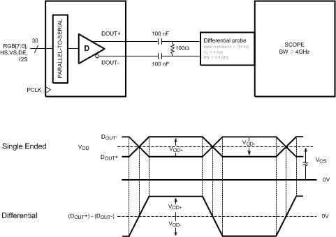 Figure 1. Serializer VOD DC Output
 Figure 2. Checkboard Data Pattern
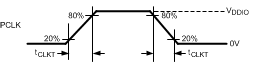 Figure 3. Serializer Input Clock Transition Time
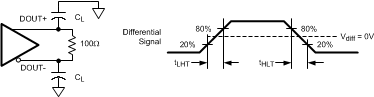 Figure 4. Serializer CML Output Load and Transition Time
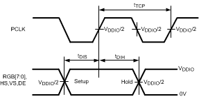 Figure 5. Serializer Setup and Hold Times
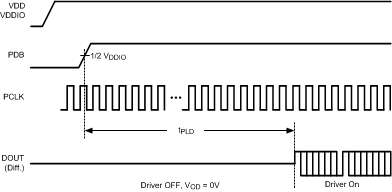 Figure 6. Serializer Lock Time
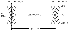 Figure 7. Serializer CML Output Jitter
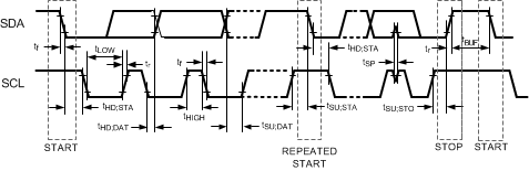 Figure 8. Serial Control Bus Timing Diagram
6.9 Switching Characteristics
over operating free-air temperature range (unless otherwise noted)| PARAMETER | TEST CONDITIONS | MIN | TYP | MAX | UNIT | ||
|---|---|---|---|---|---|---|---|
| tLHT | CML Output Low-to-High Transition Time | See Figure 4 | DOUT+, DOUT- | 80 | 130 | ps | |
| tHLT | CML Output High-to-Low Transition Time | 80 | 130 | ps | |||
| tDIS | Data Input Setup to PCLK | See Figure 5 | R[7:0], G[7:0], B[7:0], HS, VS, DE, PCLK, I2S_CLK, I2S_WC, I2S_DA, I2S_DB | 2.0 | ns | ||
| tDIH | Data Input Hold from PCLK | 2.0 | ns | ||||
| tPLD | Serializer PLL Lock Time | Figure 6(4) | f = 5 – 85 MHz | 131*T | ns | ||
| tSD | Delay — Latency | f = 5 – 85 MHz | 145*T | ns | |||
| tTJIT | Output Total Jitter, Bit Error Rate ≥10-10 Figure 7(6)(7)(5) |
RL = 100Ω f = 85MHz, LFMODE = L |
DOUT+, DOUT- | 0.25 | 0.30 | UI | |
| RL = 100Ω f = 5MHz, LFMODE = H |
0.25 | 0.30 | UI | ||||
6.10 Typical Charateristics
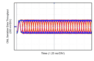
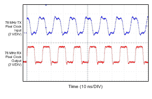
| Note: On the rising edge of each clock period, the CML driver outputs a low Stop bit, high Start bit, and 33 DC-scrambled data bits. | ||
with 78 MHZ TX Pixel Clock