SBOS154B September 2000 – April 2024 INA117
PRODUCTION DATA
- 1
- 1 Features
- 2 Applications
- 3 Description
- 4 Pin Configuration and Functions
- 5 Specifications
- 6 Typical Characteristics
- 7 Application and Implementation
- 8 Device and Documentation Support
- 9 Revision History
- 10Mechanical, Packaging, and Orderable Information
Package Options
Refer to the PDF data sheet for device specific package drawings
Mechanical Data (Package|Pins)
- D|8
- P|8
- LMC|8
Thermal pad, mechanical data (Package|Pins)
Orderable Information
7.1.3 Measuring Current
The INA117 can be used to measure a current by sensing the voltage drop across a series resistor, RS. Figure 7-4 shows the INA117 used to measure the supply currents of a device under test. The circuit in Figure 7-5 measures the output current of a power supply. If the power supply has a sense connection, the power supply can be connected to the output side of RS to eliminate the voltage-drop error. Another common application is current-to-voltage conversion, as shown in Figure 7-6.
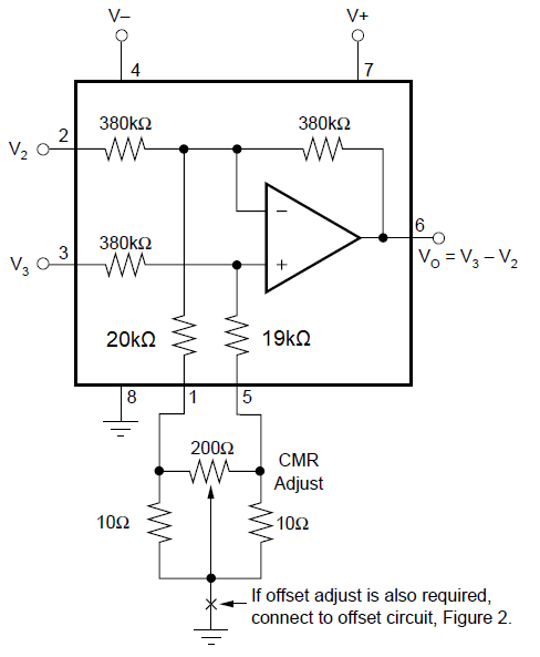 Figure 7-3 CMR Trim Circuit
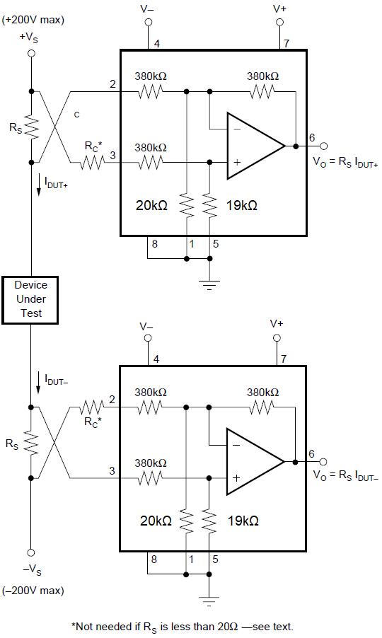 Figure 7-4 Measuring Supply Currents of
Device Under Test
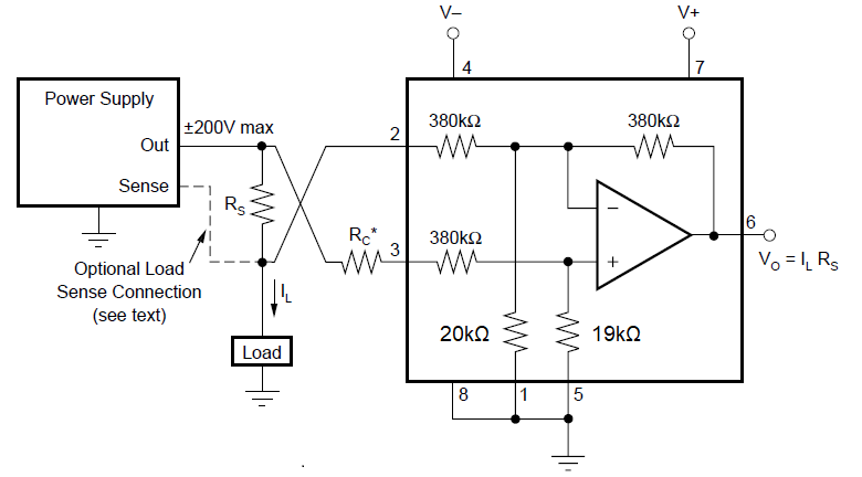
| *RC not needed if RS is less than 20Ω – see text. |
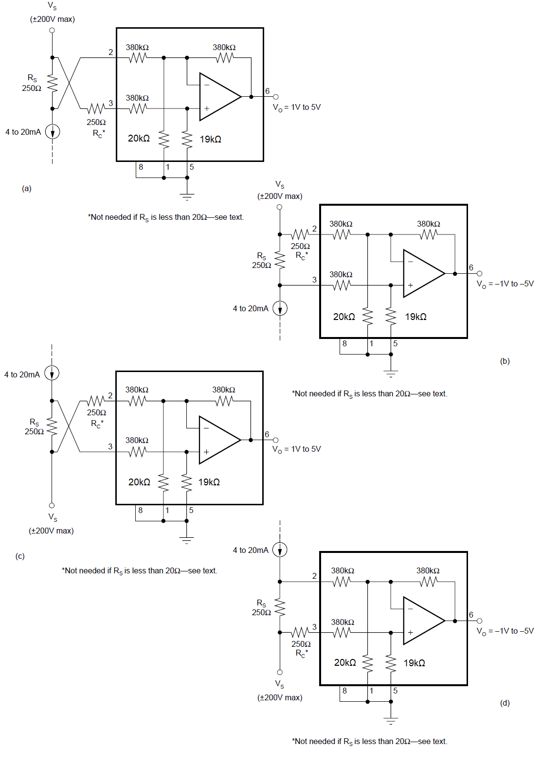 Figure 7-6 Current to Voltage
Converter
Figure 7-6 Current to Voltage
ConverterIn all cases, the sense resistor imbalances the input resistor matching of the INA117, degrading the CMR. Also, the input impedance of the INA117 loads RS, causing gain error in the voltage-to-current conversion. Both of these errors can be easily corrected.
The CMR error can be corrected with the addition of a compensation resistor, RC, equal in value to RS as shown in Figure 7-4, Figure 7-5, and Figure 7-6. If RS is less than 20Ω, the degradation in CMR is negligible and RC can be omitted. If RS is larger than approximately 2kΩ, trimming RC can be required to achieve greater than 86dB CMR. This trim is because the actual INA117 input impedances have 1% typical mismatch. If RS is more than approximately 100Ω, the gain error is greater than the 0.05% specification of the INA117. This gain error can be corrected by slightly increasing the value of RS. The corrected value, RS', can be calculated by:
Example: For a 1V/mA transfer function, the nominal, uncorrected value for RS is 1kΩ. A slightly larger value, RS' = 1002.6Ω, compensates for the gain error due to loading.
The 380kΩ term in the equation for RS' has a tolerance of ±25%, so sense resistors above approximately 400Ω can require trimming to achieve gain accuracy better than 0.05%.
Of course, if a buffer amplifier is added as shown in Figure 7-7, both inputs see a low source impedance, and the sense resistor is not loaded. As a result, there is no gain error or CMR degradation. The buffer amplifier can operate as a unity gain buffer or as an amplifier with non-inverting gain. Gain added ahead of the INA117 improves both CMR and signal-to-noise. Added gain also allows a lower voltage drop across the sense resistor. The OPA1013 is a good choice for the buffer amplifier since both the input and output can swing close to the negative power supply.
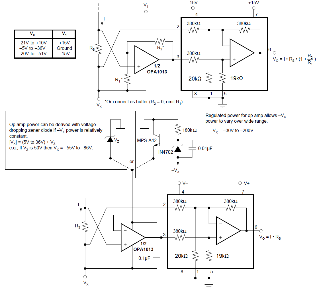 Figure 7-7 Current Sensing With Input
Buffer
Figure 7-7 Current Sensing With Input
BufferFigure 7-8 shows very high input impedance buffer used to measure low leakage currents. Here, the buffer operational amplifier is powered with an isolated, split-voltage power supply. Using an isolated power supply allows full ±200V common-mode input range.