SBOS793H April 2017 – November 2023 INA181 , INA2181 , INA4181
PRODUCTION DATA
- 1
- 1 Features
- 2 Applications
- 3 Description
- 4 Device Comparison
- 5 Pin Configuration and Functions
- 6 Specifications
- 7 Detailed Description
- 8 Application and Implementation
- 9 Device and Documentation Support
- 10Revision History
- 11Mechanical, Packaging, and Orderable Information
Package Options
Mechanical Data (Package|Pins)
Thermal pad, mechanical data (Package|Pins)
- DCK|6
Orderable Information
8.1.3 Signal Filtering
Provided that the INAx181 output is connected to a high-impedance input, the best location to filter is at the device output using a simple RC network from OUT to GND. Filtering at the output attenuates high-frequency disturbances in the common-mode voltage, differential input signal, and INAx181 power-supply voltage. If filtering at the output is not possible, or filtering of only the differential input signal is required, required, then apply a filter at the input pins of the device. Figure 8-2 provides an example of how a filter can be used on the input pins of the device.
 Figure 8-2 Filter at Input Pins
The addition of external series resistance creates an additional error in the measurement; therefore, the value of these series resistors must be kept to 10 Ω (or less, if possible) to reduce impact to accuracy. The internal bias network shown in Figure 8-2 present at the input pins creates a mismatch in input bias currents when a differential voltage is applied between the input pins. If additional external series filter resistors are added to the circuit, the mismatch in bias currents results in a mismatch of voltage drops across the filter resistors. This mismatch creates a differential error voltage that subtracts from the voltage developed across the shunt resistor. This error results in a voltage at the device input pins that is different than the voltage developed across the shunt resistor. Without the additional series resistance, the mismatch in input bias currents has little effect on device operation. The amount of error these external filter resistors add to the measurement can be calculated using Equation 6, where the gain error factor is calculated using Equation 5.
The amount of variance in the differential voltage present at the device input relative to the voltage developed at the shunt resistor is based both on the external series resistance (RF) value as well as internal input resistor RINT, as shown in Figure 8-2. The reduction of the shunt voltage reaching the device input pins appears as a gain error when comparing the output voltage relative to the voltage across the shunt resistor. A factor can be calculated to determine the amount of gain error that is introduced by the addition of external series resistance. Calculate the expected deviation from the shunt voltage to what is measured at the device input pins is given using Equation 5:
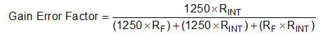
where:
- RINT is the internal input resistor.
- RF is the external series resistance.
With the adjustment factor from Equation 5, including the device internal input resistance, this factor varies with each gain version, as shown in Table 8-1. Each individual device gain error factor is shown in Table 8-2.
| PRODUCT | GAIN | RINT (kΩ) |
|---|---|---|
| INAx181A1 | 20 | 25 |
| INAx181A2 | 50 | 10 |
| INAx181A3 | 100 | 5 |
| INAx181A4 | 200 | 2.5 |
| PRODUCT | SIMPLIFIED GAIN ERROR FACTOR |
|---|---|
| INAx181A1 | 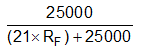 |
| INAx181A2 | 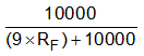 |
| INAx181A3 |  |
| INAx181A4 | 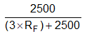 |
The gain error that can be expected from the addition of the external series resistors can then be calculated based on Equation 6:

For example, using an INA181A2 and the corresponding gain error equation from Table 8-2, a series resistance of 10 Ω results in a gain error factor of 0.991. The corresponding gain error is then calculated using Equation 6, resulting in an additional gain error of approximately 0.89% solely because of the external 10-Ω series resistors.