SBOS378A March 2019 – November 2023 INA185
PRODUCTION DATA
- 1
- 1 Features
- 2 Applications
- 3 Description
- 4 Pin Configuration and Functions
- 5 Specifications
- 6 Detailed Description
- 7 Application and Implementation
- 8 Device and Documentation Support
- 9 Revision History
- 10Mechanical, Packaging, and Orderable Information
Package Options
Mechanical Data (Package|Pins)
Thermal pad, mechanical data (Package|Pins)
Orderable Information
6.4.5 Shutdown Mode
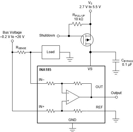
Although the INA185 does not have a shutdown pin, the low power consumption of these devices allows the output of a logic gate or transistor switch to power the INA185. This gate or switch turns on and off the INA185 power-supply quiescent current.
However, in current shunt monitoring applications, the amount of current drained from the shunt circuit in shutdown conditions is also a concern. Evaluating this current drain involves considering the simplified schematic of the INA185 in shutdown mode, as shown in Figure 6-4.
 Figure 6-4 Basic Circuit to Shut Down the INA185 With a Grounded Reference
There is typically more than 500 kΩ of impedance (from the combination of 500-kΩ feedback and
input gain set resistors) from each input of the INA185 to the OUT pin and to the REF pin. The amount of current flowing through these pins depends on the voltage at the connection. For example, if the REF pin is grounded, the calculation of the effect of the 500 kΩ impedance from the shunt to ground is straightforward. However, if the reference is powered while the INA185 is in shutdown mode, the input current will be determined by the 500-kΩ impedance and the voltage difference between the positive input and the voltage applied to the REF pin.
Regarding the 500-kΩ path to the output pin, the output stage of a disabled INA185 does constitute a good path to ground. Consequently, this current is directly proportional to a shunt common-mode voltage present across a 500-kΩ resistor.
As long as the shunt common-mode voltage is greater than VS when the device is powered up, there is an additional and well-matched 55-µA typical current that flows in each of the inputs. If less than VS, the common-mode input currents are negligible, and the only current effects are the result of the 500-kΩ resistors.