SBOS378A March 2019 – November 2023 INA185
PRODUCTION DATA
- 1
- 1 Features
- 2 Applications
- 3 Description
- 4 Pin Configuration and Functions
- 5 Specifications
- 6 Detailed Description
- 7 Application and Implementation
- 8 Device and Documentation Support
- 9 Revision History
- 10Mechanical, Packaging, and Orderable Information
Package Options
Mechanical Data (Package|Pins)
Thermal pad, mechanical data (Package|Pins)
Orderable Information
3 Description
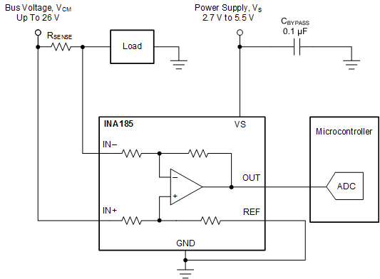
The INA185 current sense amplifier is designed for use in cost-sensitive space constrained applications. This device is a bidirectional, current-sense amplifier (also called a current-shunt monitor) that senses the voltage drop across a current-sense resistor at common-mode voltages from –0.2 V to +26 V, independent of the supply voltage. The INA185 integrates a matched resistor gain network in four, fixed-gain device options: 20 V/V, 50 V/V, 100 V/V, or 200 V/V. This matched gain resistor network minimizes gain error and reduces the temperature drift.
The INA185 operates from a single 2.7-V to 5.5-V power supply. The device draws a maximum supply current of 260 µA and features high slew rate and bandwidth making this device an excellent choice for many power-supply and motor-control applications.
The INA185 is available in an industry standard SC70 package and low profile 6-pin, SOT-563 package. The SOT-563 package has a body size of size of only 2.56 mm2, including the device pins. All device options are specified over the extended operating temperature range of –40°C to +125°C.
| PART NUMBER | PACKAGE(1) | PACKAGE SIZE(2) |
|---|---|---|
| INA185 | DRL (SOT-563, 6) | 1.60 mm × 1.60 mm |
| DCK (SC70, 6) | 2.00 mm × 2.10 mm |
 Typical Application Circuit