SBOS871A May 2019 – March 2022 INA190-Q1
PRODUCTION DATA
- 1 Features
- 2 Applications
- 3 Description
- 4 Revision History
- 5 Pin Configuration and Functions
- 6 Specifications
- 7 Detailed Description
- 8 Application and Implementation
- 9 Power Supply Recommendations
- 10Layout
- 11Device and Documentation Support
- 12Mechanical, Packaging, and Orderable Information
Package Options
Mechanical Data (Package|Pins)
Thermal pad, mechanical data (Package|Pins)
- DCK|6
Orderable Information
3 Description
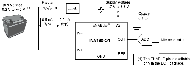
The INA190-Q1 is an automotive, low-power, voltage-output, current-shunt monitor (also called a current-sense amplifier). This device is commonly used for monitoring systems directly connected to an automotive 12-V battery. The INA190-Q1 can sense drops across shunts at common-mode voltages from –0.2 V to +40 V, independent of the supply voltage. In addition, the input pins have an absolute maximum voltage of 42 V.
The low input bias current of the device permits the use of larger current-sense resistors, thus providing accurate current measurements in the microamp range. The low offset voltage of the zero-drift architecture extends the dynamic range of the current measurement. This feature allows for smaller sense resistors with lower power loss, while still providing accurate current measurements.
The INA190-Q1 operates from a single 1.7-V to 5.5-V power supply, and draws a maximum of 65 µA of supply current when enabled; only 0.1 µA when disabled. Five fixed gain options are available: 25 V/V, 50 V/V, 100 V/V, 200 V/V, or 500 V/V. The device is specified over the operating temperature range of –40°C to +125°C, and offered in SC70 and SOT-23 packages.
| PART NUMBER | PACKAGE | BODY SIZE (NOM) |
|---|---|---|
| INA190-Q1 | SC70 (6) | 2.00 mm x 1.25 mm |
| SOT-23 (8) | 1.60 mm × 2.90 mm |
 Typical Application