SBOS776C March 2016 – March 2021 INA3221-Q1
PRODUCTION DATA
- 1 Features
- 2 Applications
- 3 Description
- 4 Revision History
- 5 Device Comparison Table
- 6 Pin Configuration and Functions
- 7 Specifications
-
8 Detailed Description
- 8.1 Overview
- 8.2 Functional Block Diagram
- 8.3 Feature Description
- 8.4 Device Functional Modes
- 8.5 Programming
- 8.6
Register Maps
- 8.6.1 Summary of Register Set
- 8.6.2
Register Descriptions
- 8.6.2.1 Configuration Register (address = 00h) [reset = 7127h]
- 8.6.2.2 Channel-1 Shunt-Voltage Register (address = 01h), [reset = 00h]
- 8.6.2.3 Channel-1 Bus-Voltage Register (address = 02h) [reset = 00h]
- 8.6.2.4 Channel-2 Shunt-Voltage Register (address = 03h) [reset = 00h]
- 8.6.2.5 Channel-2 Bus-Voltage Register (address = 04h) [reset = 00h]
- 8.6.2.6 Channel-3 Shunt-Voltage Register (address = 05h) [reset = 00h]
- 8.6.2.7 Channel-3 Bus-Voltage Register (address = 06h) [reset = 00h]
- 8.6.2.8 Channel-1 Critical-Alert Limit Register (address = 07h) [reset = 7FF8h]
- 8.6.2.9 Warning-Alert Channel-1 Limit Register (address = 08h) [reset = 7FF8h]
- 8.6.2.10 Channel-2 Critical-Alert Limit Register (address = 09h) [reset = 7FF8h]
- 8.6.2.11 Channel-2 Warning-Alert Limit Register (address = 0Ah) [reset = 7FF8h]
- 8.6.2.12 Channel-3 Critical-Alert Limit Register (address = 0Bh) [reset = 7FF8h]
- 8.6.2.13 Channel-3 Warning-Alert Limit Register (address = 0Ch) [reset = 7FF8h]
- 8.6.2.14 Shunt-Voltage Sum Register (address = 0Dh) [reset = 00h]
- 8.6.2.15 Shunt-Voltage Sum-Limit Register (address = 0Eh) [reset = 7FFEh]
- 8.6.2.16 Mask/Enable Register (address = 0Fh) [reset = 0002h]
- 8.6.2.17 Power-Valid Upper-Limit Register (address = 10h) [reset = 2710h]
- 8.6.2.18 Power-Valid Lower-Limit Register (address = 11h) [reset = 2328h]
- 8.6.2.19 Manufacturer ID Register (address = FEh) [reset = 5449h]
- 8.6.2.20 Die ID Register (address = FFh) [reset = 3220]
- 9 Application and Implementation
- 10Power Supply Recommendations
- 11Layout
- 12Device and Documentation Support
- 13Mechanical, Packaging, and Orderable Information
Package Options
Mechanical Data (Package|Pins)
- RGV|16
Thermal pad, mechanical data (Package|Pins)
Orderable Information
8.4.1 Averaging Function
The INA3221-Q1 includes three channels to monitor up to three independent supply buses; however, multichannel monitoring sometimes results in poor shunt-resistor placement. Ideally, shunt resistors are placed as close as possible to the corresponding channel input pins. However, because of system layout and multiple power-supply rails, one or more shunt resistors may have to be located further away, thus presenting potentially larger measurement errors. These errors result from additional trace inductance and other parasitic impedances between the shunt resistor and input pins. Longer traces also create an additional potential for coupling noise into the signal if they are routed near noise-generating sections of the board.
The INA3221-Q1 averaging function mitigates this potential problem by limiting the impact that any single measurement has on the averaged value of each measured signal. This limitation reduces the influence that noise has on the averaged value, thereby effectively creating an input-signal filter.
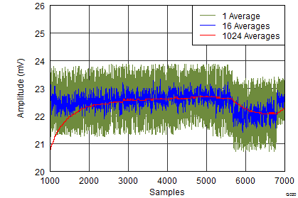
The averaging function is illustrated in Figure 8-5. Operation begins by first measuring the shunt input signal on channel 1. This value is then subtracted from the previous value that was present in the corresponding data output register. This difference is then divided by the value programmed by the averaging mode setting (AVG2-0, Configuration register bits 11-9) and stored in an internal accumulation register. The computed result is then added to the previously-loaded data output register value, and the resulting value is loaded to the corresponding data output register. After the update, the next signal to be measured follows the same process. The larger the value selected for the averaging mode setting, the less impact or influence any new conversion has on the average value, as shown in Figure 8-6. This averaging feature functions as a filter to reduce input noise from the averaged measurement value.
 Figure 8-5 Averaging Function Block Diagram
 Figure 8-6 Average Setting Example