SBOS776C March 2016 – March 2021 INA3221-Q1
PRODUCTION DATA
- 1 Features
- 2 Applications
- 3 Description
- 4 Revision History
- 5 Device Comparison Table
- 6 Pin Configuration and Functions
- 7 Specifications
-
8 Detailed Description
- 8.1 Overview
- 8.2 Functional Block Diagram
- 8.3 Feature Description
- 8.4 Device Functional Modes
- 8.5 Programming
- 8.6
Register Maps
- 8.6.1 Summary of Register Set
- 8.6.2
Register Descriptions
- 8.6.2.1 Configuration Register (address = 00h) [reset = 7127h]
- 8.6.2.2 Channel-1 Shunt-Voltage Register (address = 01h), [reset = 00h]
- 8.6.2.3 Channel-1 Bus-Voltage Register (address = 02h) [reset = 00h]
- 8.6.2.4 Channel-2 Shunt-Voltage Register (address = 03h) [reset = 00h]
- 8.6.2.5 Channel-2 Bus-Voltage Register (address = 04h) [reset = 00h]
- 8.6.2.6 Channel-3 Shunt-Voltage Register (address = 05h) [reset = 00h]
- 8.6.2.7 Channel-3 Bus-Voltage Register (address = 06h) [reset = 00h]
- 8.6.2.8 Channel-1 Critical-Alert Limit Register (address = 07h) [reset = 7FF8h]
- 8.6.2.9 Warning-Alert Channel-1 Limit Register (address = 08h) [reset = 7FF8h]
- 8.6.2.10 Channel-2 Critical-Alert Limit Register (address = 09h) [reset = 7FF8h]
- 8.6.2.11 Channel-2 Warning-Alert Limit Register (address = 0Ah) [reset = 7FF8h]
- 8.6.2.12 Channel-3 Critical-Alert Limit Register (address = 0Bh) [reset = 7FF8h]
- 8.6.2.13 Channel-3 Warning-Alert Limit Register (address = 0Ch) [reset = 7FF8h]
- 8.6.2.14 Shunt-Voltage Sum Register (address = 0Dh) [reset = 00h]
- 8.6.2.15 Shunt-Voltage Sum-Limit Register (address = 0Eh) [reset = 7FFEh]
- 8.6.2.16 Mask/Enable Register (address = 0Fh) [reset = 0002h]
- 8.6.2.17 Power-Valid Upper-Limit Register (address = 10h) [reset = 2710h]
- 8.6.2.18 Power-Valid Lower-Limit Register (address = 11h) [reset = 2328h]
- 8.6.2.19 Manufacturer ID Register (address = FEh) [reset = 5449h]
- 8.6.2.20 Die ID Register (address = FFh) [reset = 3220]
- 9 Application and Implementation
- 10Power Supply Recommendations
- 11Layout
- 12Device and Documentation Support
- 13Mechanical, Packaging, and Orderable Information
Package Options
Mechanical Data (Package|Pins)
- RGV|16
Thermal pad, mechanical data (Package|Pins)
Orderable Information
8.4.2.2 Averaging and Conversion-Time Considerations
The INA3221-Q1 has programmable conversion times for both the shunt- and bus-voltage measurements. The selectable conversion times for these measurements range from 140 μs to 8.244 ms. The conversion-time settings, along with the programmable-averaging mode, enable the INA3221-Q1 to optimize available timing requirements in a given application. For example, if a system requires data to be read every 2 ms with all three channels monitored, configure the INA3221-Q1 with the conversion times for the shunt- and bus-voltage measurements set to 332 μs.
The INA3221-Q1 can also be configured with a different conversion-time setting for the shunt- and bus-voltage measurements. This approach is common in applications where the bus voltage tends to be relatively stable, and allows for the time focused on the bus voltage measurement to be reduced relative to the shunt-voltage measurement. For example, the shunt-voltage conversion time can be set to 4.156 ms with the bus-voltage conversion time set to 588 μs for a 5-ms update time.
There are trade-offs associated with the conversion-time and averaging-mode settings. The averaging feature significantly improves the measurement accuracy by effectively filtering the signal. This approach allows the INA3221-Q1 to reduce the amount of noise in the measurement caused by noise coupling into the signal. A greater number of averages allows the INA3221-Q1 to be more effective in reducing the measurement noise component. The trade-off to this noise reduction is that the averaged value has a longer response time to input-signal changes. This aspect of the averaging feature is mitigated to some extent with the critical-alert feature that compares each single conversion to determine if a measured signal (with noise component) has exceeded the maximum acceptable level.
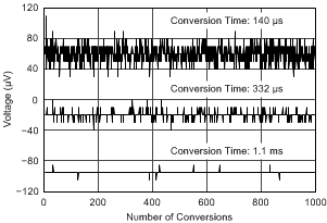
The selected conversion times also have an impact on measurement accuracy. This effect can seen in Figure 8-7. The multiple conversion times shown in Figure 8-7 illustrate the impact of noise on measurement. These curves shown do not use averaging. In order to achieve the highest-accuracy measurement possible, use a combination of the longest allowable conversion times and highest number of averages, based on system timing requirements.
 Figure 8-7 Noise Versus Conversion Time